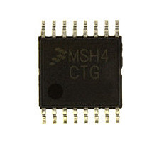
MC9S08SH4CTG Freescale, MC9S08SH4CTG Datasheet - Page 77

MC9S08SH4CTG
Manufacturer Part Number
MC9S08SH4CTG
Description
Manufacturer
Freescale
Datasheet
1.MC9S08SH4CTG.pdf
(338 pages)
Specifications of MC9S08SH4CTG
Cpu Family
HCS08
Device Core Size
8b
Frequency (max)
40MHz
Interface Type
I2C/SCI/SPI
Total Internal Ram Size
256Byte
# I/os (max)
13
Number Of Timers - General Purpose
1
Operating Supply Voltage (typ)
3.3/5V
Operating Supply Voltage (max)
5.5V
Operating Supply Voltage (min)
2.7V
On-chip Adc
8-chx10-bit
Instruction Set Architecture
CISC
Operating Temp Range
-40C to 85C
Operating Temperature Classification
Industrial
Mounting
Surface Mount
Pin Count
16
Package Type
TSSOP
Program Memory Type
Flash
Program Memory Size
4KB
Lead Free Status / RoHS Status
Compliant
Available stocks
Company
Part Number
Manufacturer
Quantity
Price
Company:
Part Number:
MC9S08SH4CTG
Manufacturer:
FREESCAL
Quantity:
96
Company:
Part Number:
MC9S08SH4CTG
Manufacturer:
Freescale
Quantity:
8 727
- Current page: 77 of 338
- Download datasheet (4Mb)
1
2
6.3
The MC9S08SH8 devices contain a feature that allows for up to eight port pins to be tied together
externally to allow higher output current drive. The ganged output drive control register (GNGC) is a
write-once register that is used to enabled the ganged output feature and select which port pins will be used
as ganged outputs. The GNGEN bit in GNGC enables ganged output. The GNGPS[7:1] bits are used to
select which pin will be part of the ganged output.
When GNGEN is set, any pin that is enabled as a ganged output will be automatically configured as an
output and follow the data, drive strength and slew rate control of PTC0. The ganged output drive pin
mapping is shown in
Freescale Semiconductor
Drive Strength
Data Direction
Ganged output not available on 8-pin packages. PTC3-PTC0 not available on 16-pin packages, however PTC0 control
registers are still used to control ganged output.
When GNGEN = 1, PTC0 is forced to an output, regardless of the value in PTCDD0 in PTCDD.
Slew Rate
Port Pin
Control
Control
Control
Control
Data
Ganged Output
2
See the DC characteristics in the electrical section for maximum Port I/O
currents allowed for this MCU.
When a pin is enabled as ganged output, this feature will have priority over
any digital module. An enabled analog function will have priority over the
ganged output pin. See
GNGPS7
PTB5
Table
6-1.
Pin is automatically configured as output when pin is enabled as ganged output.
GNGPS6
PTB4
MC9S08SH8 MCU Series Data Sheet, Rev. 3
Table 6-1. Ganged Output Pin Enable
Table 2-1
PTCDS0 in PTCDS controls drive stength of output
GNGPS5
PTCSE0 in PTCSE controls slew rate of output
PTB3
PTCD0 in PTCD controls data value of output
for information on pin priority. .
NOTE
GNGPS4
GNGC Register Bits
PTB2
GNGPS3
PTC3
GNGPS2
Chapter 6 Parallel Input/Output Control
PTC2
GNGPS1
PTC1
GNGEN
PTC0
1
77
Related parts for MC9S08SH4CTG
Image
Part Number
Description
Manufacturer
Datasheet
Request
R

Part Number:
Description:
TOWER ELEVATOR BOARDS HARDWARE
Manufacturer:
Freescale Semiconductor
Datasheet:

Part Number:
Description:
TOWER SERIAL I/O HARDWARE
Manufacturer:
Freescale Semiconductor
Datasheet:

Part Number:
Description:
LCD MODULE FOR TWR SYSTEM
Manufacturer:
Freescale Semiconductor
Datasheet:

Part Number:
Description:
DAUGHTER LCD WVGA I.MX51
Manufacturer:
Freescale Semiconductor
Datasheet:

Part Number:
Description:
TOWER SYSTEM BOARD MPC5125
Manufacturer:
Freescale Semiconductor
Datasheet:

Part Number:
Description:
KIT EVALUATION I.MX51
Manufacturer:
Freescale Semiconductor
Datasheet:

Part Number:
Description:
KIT DEVELOPMENT WINCE IMX25
Manufacturer:
Freescale Semiconductor
Datasheet:

Part Number:
Description:
TOWER SYSTEM KIT MPC5125
Manufacturer:
Freescale Semiconductor
Datasheet:

Part Number:
Description:
TOWER SYSTEM BOARD K40X256
Manufacturer:
Freescale Semiconductor
Datasheet:

Part Number:
Description:
TOWER SYSTEM KIT K40X256
Manufacturer:
Freescale Semiconductor
Datasheet:

Part Number:
Description:
Microcontrollers (MCU) MX28 PLATFORM DEV KIT
Manufacturer:
Freescale Semiconductor
Datasheet:

Part Number:
Description:
MCU, MPU & DSP Development Tools IAR KickStart Kit for Kinetis K60
Manufacturer:
Freescale Semiconductor
Datasheet:

Part Number:
Description:
24BIT HDMI MX535/08
Manufacturer:
Freescale Semiconductor
Datasheet:
Part Number:
Description:
Manufacturer:
Freescale Semiconductor, Inc
Datasheet:
Part Number:
Description:
Manufacturer:
Freescale Semiconductor, Inc
Datasheet:


