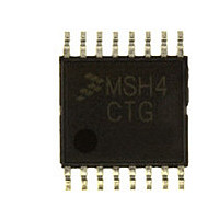
MC9S08SH4CTG Freescale, MC9S08SH4CTG Datasheet - Page 91

MC9S08SH4CTG
Manufacturer Part Number
MC9S08SH4CTG
Description
Manufacturer
Freescale
Datasheet
1.MC9S08SH4CTG.pdf
(338 pages)
Specifications of MC9S08SH4CTG
Cpu Family
HCS08
Device Core Size
8b
Frequency (max)
40MHz
Interface Type
I2C/SCI/SPI
Total Internal Ram Size
256Byte
# I/os (max)
13
Number Of Timers - General Purpose
1
Operating Supply Voltage (typ)
3.3/5V
Operating Supply Voltage (max)
5.5V
Operating Supply Voltage (min)
2.7V
On-chip Adc
8-chx10-bit
Instruction Set Architecture
CISC
Operating Temp Range
-40C to 85C
Operating Temperature Classification
Industrial
Mounting
Surface Mount
Pin Count
16
Package Type
TSSOP
Program Memory Type
Flash
Program Memory Size
4KB
Lead Free Status / RoHS Status
Compliant
Available stocks
Company
Part Number
Manufacturer
Quantity
Price
Company:
Part Number:
MC9S08SH4CTG
Manufacturer:
FREESCAL
Quantity:
96
Company:
Part Number:
MC9S08SH4CTG
Manufacturer:
Freescale
Quantity:
8 727
- Current page: 91 of 338
- Download datasheet (4Mb)
6.6.3.5
6.6.3.6
Freescale Semiconductor
PTCDS[3:0]
GNGP[7:1]
Reset:
Reset:
GNGEN
Field
Field
3:0
7:1
0
W
W
R
R
GNGPS7
Output Drive Strength Selection for Port C Bits — Each of these control bits selects between low and high
output drive for the associated PTC pin. For port C pins that are configured as inputs, these bits have no effect.
0 Low output drive strength selected for port C bit n.
1 High output drive strength selected for port C bit n.
Ganged Output Pin Select Bits— These write-once control bits selects whether the associated pin (see
Table
be controlled by the data, drive strength and slew rate settings for PTCO.
0 Associated pin is not part of the ganged output drive.
1 Assoicated pin is part of the ganged output drive. Requires GNGEN = 1.
Ganged Output Drive Enable Bit— This write-once control bit selects whether the ganged output drive feature
is enabled.
0 Ganged output drive disabled.
1 Ganged output drive enabled. PTC0 forced to output regardless of the value of PTCDD0 in PTCDD.
Port C Drive Strength Selection Register (PTCDS)
0
0
Ganged Output Drive Control Register (GNGC)
0
7
7
6-1for pins available) is enabled for ganged output. When GNGEN = 1, all enabled ganged output pins will
Figure 6-23. Drive Strength Selection for Port C Register (PTCDS)
GNGPS6
Figure 6-24. Ganged Output Drive Control Register (GNGC)
0
0
0
6
6
Table 6-22. PTCDS Register Field Descriptions
Table 6-23. GNGC Register Field Descriptions
MC9S08SH8 MCU Series Data Sheet, Rev. 3
GNGPS5
0
0
0
5
5
GNGPS4
0
0
0
4
4
Description
Description
GNGPS3
PTCDS3
3
0
3
0
GNGPS2
PTCDS2
Chapter 6 Parallel Input/Output Control
0
0
2
2
GNGPS1
PTCDS1
0
0
1
1
PTCDS0
GNGEN
0
0
0
0
91
Related parts for MC9S08SH4CTG
Image
Part Number
Description
Manufacturer
Datasheet
Request
R

Part Number:
Description:
TOWER ELEVATOR BOARDS HARDWARE
Manufacturer:
Freescale Semiconductor
Datasheet:

Part Number:
Description:
TOWER SERIAL I/O HARDWARE
Manufacturer:
Freescale Semiconductor
Datasheet:

Part Number:
Description:
LCD MODULE FOR TWR SYSTEM
Manufacturer:
Freescale Semiconductor
Datasheet:

Part Number:
Description:
DAUGHTER LCD WVGA I.MX51
Manufacturer:
Freescale Semiconductor
Datasheet:

Part Number:
Description:
TOWER SYSTEM BOARD MPC5125
Manufacturer:
Freescale Semiconductor
Datasheet:

Part Number:
Description:
KIT EVALUATION I.MX51
Manufacturer:
Freescale Semiconductor
Datasheet:

Part Number:
Description:
KIT DEVELOPMENT WINCE IMX25
Manufacturer:
Freescale Semiconductor
Datasheet:

Part Number:
Description:
TOWER SYSTEM KIT MPC5125
Manufacturer:
Freescale Semiconductor
Datasheet:

Part Number:
Description:
TOWER SYSTEM BOARD K40X256
Manufacturer:
Freescale Semiconductor
Datasheet:

Part Number:
Description:
TOWER SYSTEM KIT K40X256
Manufacturer:
Freescale Semiconductor
Datasheet:

Part Number:
Description:
Microcontrollers (MCU) MX28 PLATFORM DEV KIT
Manufacturer:
Freescale Semiconductor
Datasheet:

Part Number:
Description:
MCU, MPU & DSP Development Tools IAR KickStart Kit for Kinetis K60
Manufacturer:
Freescale Semiconductor
Datasheet:

Part Number:
Description:
24BIT HDMI MX535/08
Manufacturer:
Freescale Semiconductor
Datasheet:
Part Number:
Description:
Manufacturer:
Freescale Semiconductor, Inc
Datasheet:
Part Number:
Description:
Manufacturer:
Freescale Semiconductor, Inc
Datasheet:


