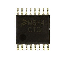
MC9S08SH4CTG Freescale, MC9S08SH4CTG Datasheet - Page 78

MC9S08SH4CTG
Manufacturer Part Number
MC9S08SH4CTG
Description
Manufacturer
Freescale
Datasheet
1.MC9S08SH4CTG.pdf
(338 pages)
Specifications of MC9S08SH4CTG
Cpu Family
HCS08
Device Core Size
8b
Frequency (max)
40MHz
Interface Type
I2C/SCI/SPI
Total Internal Ram Size
256Byte
# I/os (max)
13
Number Of Timers - General Purpose
1
Operating Supply Voltage (typ)
3.3/5V
Operating Supply Voltage (max)
5.5V
Operating Supply Voltage (min)
2.7V
On-chip Adc
8-chx10-bit
Instruction Set Architecture
CISC
Operating Temp Range
-40C to 85C
Operating Temperature Classification
Industrial
Mounting
Surface Mount
Pin Count
16
Package Type
TSSOP
Program Memory Type
Flash
Program Memory Size
4KB
Lead Free Status / RoHS Status
Compliant
Available stocks
Company
Part Number
Manufacturer
Quantity
Price
Company:
Part Number:
MC9S08SH4CTG
Manufacturer:
FREESCAL
Quantity:
96
Company:
Part Number:
MC9S08SH4CTG
Manufacturer:
Freescale
Quantity:
8 727
- Current page: 78 of 338
- Download datasheet (4Mb)
Chapter 6 Parallel Input/Output Control
6.4
Port A[3:0] and port B[3:0] pins can be configured as external interrupt inputs and as an external means of
waking the MCU from stop3 or wait low-power modes.
The block diagram for the pin interrupts is shown
Writing to the PTxPSn bits in the port interrupt pin enable register (PTxPS) independently enables or
disables each port pin interrupt. Each port can be configured as edge sensitive or edge and level sensitive
based on the PTxMOD bit in the port interrupt status and control register (PTxSC). Edge sensitivity can
be software programmed to be either falling or rising; the level can be either low or high. The polarity of
the edge or edge and level sensitivity is selected using the PTxESn bits in the port interrupt edge select
register (PTxES).
Synchronous logic is used to detect edges. Prior to detecting an edge, enabled pin interrupt inputs must be
at the deasserted logic level. A falling edge is detected when an enabled port input signal is seen as a logic
1 (the deasserted level) during one bus cycle and then a logic 0 (the asserted level) during the next cycle.
A rising edge is detected when the input signal is seen as a logic 0 during one bus cycle and then a logic 1
during the next cycle.
6.4.1
A valid edge on an enabled pin interrupt will set PTxIF in PTxSC. If PTxIE in PTxSC is set, an interrupt
request will be presented to the CPU. Clearing of PTxIF is accomplished by writing a 1 to PTxACK in
PTxSC.
6.4.2
A valid edge or level on an enabled pin interrupt will set PTxIF in PTxSC. If PTxIE in PTxSC is set, an
interrupt request will be presented to the CPU. Clearing of PTxIF is accomplished by writing a 1 to
PTxACK in PTxSC provided all enabled pin interrupt inputs are at their deasserted levels. PTxIF will
remain set if any enabled pin interrupt is asserted while attempting to clear by writing a 1 to PTxACK.
78
PIxn
PIxn
PTxESn
PTxES0
Pin Interrupts
0
0
1
1
S
S
Edge Only Sensitivity
Edge and Level Sensitivity
PTxPSn
PTxPS0
Figure 6-2. Pin Interrupt Block Diagram
MC9S08SH8 MCU Series Data Sheet, Rev. 3
PTxMOD
V
DD
D
Figure
CK
CLR
Q
6-2.
INTERRUPT FF
PORT
PTxACK
RESET
STOP
SYNCHRONIZER
STOP BYPASS
BUSCLK
PTxIE
Freescale Semiconductor
PTxIF
PTx
INTERRUPT
REQUEST
Related parts for MC9S08SH4CTG
Image
Part Number
Description
Manufacturer
Datasheet
Request
R

Part Number:
Description:
TOWER ELEVATOR BOARDS HARDWARE
Manufacturer:
Freescale Semiconductor
Datasheet:

Part Number:
Description:
TOWER SERIAL I/O HARDWARE
Manufacturer:
Freescale Semiconductor
Datasheet:

Part Number:
Description:
LCD MODULE FOR TWR SYSTEM
Manufacturer:
Freescale Semiconductor
Datasheet:

Part Number:
Description:
DAUGHTER LCD WVGA I.MX51
Manufacturer:
Freescale Semiconductor
Datasheet:

Part Number:
Description:
TOWER SYSTEM BOARD MPC5125
Manufacturer:
Freescale Semiconductor
Datasheet:

Part Number:
Description:
KIT EVALUATION I.MX51
Manufacturer:
Freescale Semiconductor
Datasheet:

Part Number:
Description:
KIT DEVELOPMENT WINCE IMX25
Manufacturer:
Freescale Semiconductor
Datasheet:

Part Number:
Description:
TOWER SYSTEM KIT MPC5125
Manufacturer:
Freescale Semiconductor
Datasheet:

Part Number:
Description:
TOWER SYSTEM BOARD K40X256
Manufacturer:
Freescale Semiconductor
Datasheet:

Part Number:
Description:
TOWER SYSTEM KIT K40X256
Manufacturer:
Freescale Semiconductor
Datasheet:

Part Number:
Description:
Microcontrollers (MCU) MX28 PLATFORM DEV KIT
Manufacturer:
Freescale Semiconductor
Datasheet:

Part Number:
Description:
MCU, MPU & DSP Development Tools IAR KickStart Kit for Kinetis K60
Manufacturer:
Freescale Semiconductor
Datasheet:

Part Number:
Description:
24BIT HDMI MX535/08
Manufacturer:
Freescale Semiconductor
Datasheet:
Part Number:
Description:
Manufacturer:
Freescale Semiconductor, Inc
Datasheet:
Part Number:
Description:
Manufacturer:
Freescale Semiconductor, Inc
Datasheet:


