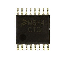
MC9S08SH4CTG Freescale, MC9S08SH4CTG Datasheet - Page 69

MC9S08SH4CTG
Manufacturer Part Number
MC9S08SH4CTG
Description
Manufacturer
Freescale
Datasheet
1.MC9S08SH4CTG.pdf
(338 pages)
Specifications of MC9S08SH4CTG
Cpu Family
HCS08
Device Core Size
8b
Frequency (max)
40MHz
Interface Type
I2C/SCI/SPI
Total Internal Ram Size
256Byte
# I/os (max)
13
Number Of Timers - General Purpose
1
Operating Supply Voltage (typ)
3.3/5V
Operating Supply Voltage (max)
5.5V
Operating Supply Voltage (min)
2.7V
On-chip Adc
8-chx10-bit
Instruction Set Architecture
CISC
Operating Temp Range
-40C to 85C
Operating Temperature Classification
Industrial
Mounting
Surface Mount
Pin Count
16
Package Type
TSSOP
Program Memory Type
Flash
Program Memory Size
4KB
Lead Free Status / RoHS Status
Compliant
Available stocks
Company
Part Number
Manufacturer
Quantity
Price
Company:
Part Number:
MC9S08SH4CTG
Manufacturer:
FREESCAL
Quantity:
96
Company:
Part Number:
MC9S08SH4CTG
Manufacturer:
Freescale
Quantity:
8 727
- Current page: 69 of 338
- Download datasheet (4Mb)
1
2
5.7.4
This high page register is a write-once register so only the first write after reset is honored. It can be read
at any time. Any subsequent attempt to write to SOPT1 (intentionally or unintentionally) is ignored to
avoid accidental changes to these sensitive settings. SOPT1 should be written during the user’s reset
initialization program to set the desired controls even if the desired settings are the same as the reset
settings.
Freescale Semiconductor
Bit 4 is reserved, writes change the value, but will have no effect on this MCU.
u = unaffected
COPT[1:0]
Reset:
BKGDPE
STOPE
RSTPE
POR:
IICPS
LVR:
Field
7:6
5
2
1
0
W
R
System Options Register 1 (SOPT1)
COP Watchdog Timeout — These write-once bits select the timeout period of the COP. COPT along with
COPCLKS in SOPT2 defines the COP timeout period. See
Stop Mode Enable — This write-once bit is used to enable stop mode. If stop mode is disabled and a user
program attempts to execute a STOP instruction, an illegal opcode reset is forced.
0 Stop mode disabled.
1 Stop mode enabled.
IIC Pin Select — This bit selects the location of the SDA and SCL pins of the IIC module.
0 SDA on PTA2, SCL on PTA3.
1 SDA on PTB6, SCL on PTB7.
Background Debug Mode Pin Enable — This write-once bit when set enables the PTA4/ACMPO/BKGD/MS
pin to function as BKGD/MS. When clear, the pin functions as one of its output-only alternative functions. This
pin defaults to the BKGD/MS function following any MCU reset.
0 PTA4/ACMPO/BKGD/MS pin functions as PTA4 or ACMPO.
1 PTA4/ACMPO/BKGD/MS pin functions as BKGD/MS.
RESET Pin Enable — This write-once bit when set enables the PTA5/IRQ/TCLK/RESET pin to function as
RESET. When clear, the pin functions as one of its alternative functions. This pin defaults to a general-purpose
input port function following a POR reset. When configured as RESET, the pin will be unaffected by LVR or other
internal resets. When RSTPE is set, an internal pullup device is enabled on RESET.
0 PTA5/IRQ/TCLK/RESET pin functions as PTA5, IRQ or TCLK.
1 PTA5/IRQ/TCLK/RESET pin functions as RESET.
1
1
1
7
COPT
= Unimplemented or Reserved
1
1
1
6
Figure 5-5. System Options Register 1 (SOPT1)
Table 5-6. SOPT1 Register Field Descriptions
MC9S08SH8 MCU Series Data Sheet, Rev. 3
STOPE
0
0
0
5
4
0
0
0
1
Description
Chapter 5 Resets, Interrupts, and General System Control
Table
3
0
0
0
0
5-1.
IICPS
0
0
0
2
BKGDPE
1
1
1
1
RSTPE
u
0
u
0
2
69
Related parts for MC9S08SH4CTG
Image
Part Number
Description
Manufacturer
Datasheet
Request
R

Part Number:
Description:
TOWER ELEVATOR BOARDS HARDWARE
Manufacturer:
Freescale Semiconductor
Datasheet:

Part Number:
Description:
TOWER SERIAL I/O HARDWARE
Manufacturer:
Freescale Semiconductor
Datasheet:

Part Number:
Description:
LCD MODULE FOR TWR SYSTEM
Manufacturer:
Freescale Semiconductor
Datasheet:

Part Number:
Description:
DAUGHTER LCD WVGA I.MX51
Manufacturer:
Freescale Semiconductor
Datasheet:

Part Number:
Description:
TOWER SYSTEM BOARD MPC5125
Manufacturer:
Freescale Semiconductor
Datasheet:

Part Number:
Description:
KIT EVALUATION I.MX51
Manufacturer:
Freescale Semiconductor
Datasheet:

Part Number:
Description:
KIT DEVELOPMENT WINCE IMX25
Manufacturer:
Freescale Semiconductor
Datasheet:

Part Number:
Description:
TOWER SYSTEM KIT MPC5125
Manufacturer:
Freescale Semiconductor
Datasheet:

Part Number:
Description:
TOWER SYSTEM BOARD K40X256
Manufacturer:
Freescale Semiconductor
Datasheet:

Part Number:
Description:
TOWER SYSTEM KIT K40X256
Manufacturer:
Freescale Semiconductor
Datasheet:

Part Number:
Description:
Microcontrollers (MCU) MX28 PLATFORM DEV KIT
Manufacturer:
Freescale Semiconductor
Datasheet:

Part Number:
Description:
MCU, MPU & DSP Development Tools IAR KickStart Kit for Kinetis K60
Manufacturer:
Freescale Semiconductor
Datasheet:

Part Number:
Description:
24BIT HDMI MX535/08
Manufacturer:
Freescale Semiconductor
Datasheet:
Part Number:
Description:
Manufacturer:
Freescale Semiconductor, Inc
Datasheet:
Part Number:
Description:
Manufacturer:
Freescale Semiconductor, Inc
Datasheet:


