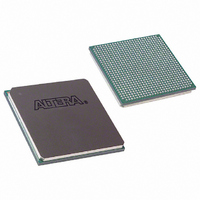
EP1S10F780I6N Altera, EP1S10F780I6N Datasheet - Page 403

EP1S10F780I6N
Manufacturer Part Number
EP1S10F780I6N
Description
IC STRATIX FPGA 10K LE 780-FBGA
Manufacturer
Altera
Series
Stratix®r
Datasheet
1.EP1S10F484I6N.pdf
(864 pages)
Specifications of EP1S10F780I6N
Number Of Logic Elements/cells
10570
Number Of Labs/clbs
1057
Total Ram Bits
920448
Number Of I /o
426
Voltage - Supply
1.425 V ~ 1.575 V
Mounting Type
Surface Mount
Operating Temperature
0°C ~ 85°C
Package / Case
780-FBGA
Lead Free Status / RoHS Status
Lead free / RoHS Compliant
Number Of Gates
-
Available stocks
Company
Part Number
Manufacturer
Quantity
Price
Company:
Part Number:
EP1S10F780I6N
Manufacturer:
ALTERA
Quantity:
3 000
- Current page: 403 of 864
- Download datasheet (11Mb)
Altera Corporation
June 2006
Interface Pins
QDR and QDRII SRAM uses two separate, uni-directional data ports for
read and write operations, enabling quad data-rate data transfer. Both
QDR and QDRII SRAM use shared address lines for reads and writes.
Stratix and Stratix GX devices utilize dedicated DDR I/O circuitry for the
input and output data bus and the K and Kn output clock signals.
Both QDR and QDRII SRAM burst-of-two devices sample the read
address on the rising edge of the K clock and sample the write address on
the rising edge of the Kn clock while QDR and QDRII SRAM burst-of-
four devices sample both read and write addresses on the K clock's rising
edge. You can use any of the Stratix and Stratix GX device user I/O pins
in I/O banks 3, 4, 7, and 8 for the D write data ports, commands, and
addresses.
QDR SRAM uses the following clock signals: input clocks K and Kn and
output clocks C and Cn. In addition to the aforementioned two pairs of
clocks, QDRII SRAM also uses echo clocks CQ and CQn. Clocks Cn, Kn,
and CQn are logical complements of clocks C, K, and CQ respectively.
Clocks C, Cn, K, and Kn are inputs to the QDRII SRAM while clocks CQ
and CQn are outputs from the QDRII SRAM. Stratix and Stratix GX
devices use single-clock mode for single-device QDR and QDRII SRAM
interfacing where the K and Kn are used for both read and write
operations, and the C and Cn clocks are unused. Use both C or Cn and K
or Kn clocks when interfacing with a bank of multiple QDRII SRAM
devices with a single controller.
You can generate C, Cn, K, and Kn clocks using any of the I/O registers
in I/O banks 3, 4, 7, or 8 via the DDR registers. Due to strict skew
requirements between K and Kn signals, use adjacent pins to generate the
clock pair. Surround the pair with buffer pins tied to V
better noise immunity from other signals.
In general, all output signals to the QDR and QDRII SRAM should use the
top and bottom banks (I/O banks 3, 4, 7, or 8). You can place the input
signals from the QDR and QDRII SRAM in any I/O banks.
Read & Write Operations
Figure 3–5
devices at the memory pins during reads. QDR and QDRII SRAM devices
send data within a t
Cn in multi-clock mode, or the input clock K or Kn in single clock mode.
Data is valid until t
shows the data and clock relationships in QDRII SRAM
External Memory Interfaces in Stratix & Stratix GX Devices
DOH
CO
time after each rising edge of the input clock C or
time, after each rising edge of the C or Cn in multi-
Stratix Device Handbook, Volume 2
CC
and ground for
3–7
Related parts for EP1S10F780I6N
Image
Part Number
Description
Manufacturer
Datasheet
Request
R

Part Number:
Description:
CYCLONE II STARTER KIT EP2C20N
Manufacturer:
Altera
Datasheet:

Part Number:
Description:
CPLD, EP610 Family, ECMOS Process, 300 Gates, 16 Macro Cells, 16 Reg., 16 User I/Os, 5V Supply, 35 Speed Grade, 24DIP
Manufacturer:
Altera Corporation
Datasheet:

Part Number:
Description:
CPLD, EP610 Family, ECMOS Process, 300 Gates, 16 Macro Cells, 16 Reg., 16 User I/Os, 5V Supply, 15 Speed Grade, 24DIP
Manufacturer:
Altera Corporation
Datasheet:

Part Number:
Description:
Manufacturer:
Altera Corporation
Datasheet:

Part Number:
Description:
CPLD, EP610 Family, ECMOS Process, 300 Gates, 16 Macro Cells, 16 Reg., 16 User I/Os, 5V Supply, 30 Speed Grade, 24DIP
Manufacturer:
Altera Corporation
Datasheet:

Part Number:
Description:
High-performance, low-power erasable programmable logic devices with 8 macrocells, 10ns
Manufacturer:
Altera Corporation
Datasheet:

Part Number:
Description:
High-performance, low-power erasable programmable logic devices with 8 macrocells, 7ns
Manufacturer:
Altera Corporation
Datasheet:

Part Number:
Description:
Classic EPLD
Manufacturer:
Altera Corporation
Datasheet:

Part Number:
Description:
High-performance, low-power erasable programmable logic devices with 8 macrocells, 10ns
Manufacturer:
Altera Corporation
Datasheet:

Part Number:
Description:
Manufacturer:
Altera Corporation
Datasheet:

Part Number:
Description:
Manufacturer:
Altera Corporation
Datasheet:

Part Number:
Description:
Manufacturer:
Altera Corporation
Datasheet:

Part Number:
Description:
CPLD, EP610 Family, ECMOS Process, 300 Gates, 16 Macro Cells, 16 Reg., 16 User I/Os, 5V Supply, 25 Speed Grade, 24DIP
Manufacturer:
Altera Corporation
Datasheet:


