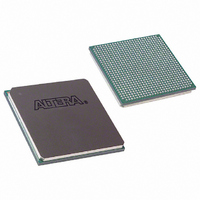
EP1S10F780I6N Altera, EP1S10F780I6N Datasheet - Page 512

EP1S10F780I6N
Manufacturer Part Number
EP1S10F780I6N
Description
IC STRATIX FPGA 10K LE 780-FBGA
Manufacturer
Altera
Series
Stratix®r
Datasheet
1.EP1S10F484I6N.pdf
(864 pages)
Specifications of EP1S10F780I6N
Number Of Logic Elements/cells
10570
Number Of Labs/clbs
1057
Total Ram Bits
920448
Number Of I /o
426
Voltage - Supply
1.425 V ~ 1.575 V
Mounting Type
Surface Mount
Operating Temperature
0°C ~ 85°C
Package / Case
780-FBGA
Lead Free Status / RoHS Status
Lead free / RoHS Compliant
Number Of Gates
-
Available stocks
Company
Part Number
Manufacturer
Quantity
Price
Company:
Part Number:
EP1S10F780I6N
Manufacturer:
ALTERA
Quantity:
3 000
- Current page: 512 of 864
- Download datasheet (11Mb)
Source-Synchronous Timing Budget
Figure 5–26. Output Timing Waveform
Note to
(1)
5–40
Stratix Device Handbook, Volume 2
Output Clock
(Differential
Signal)
Output Data
TPPos0 (max)
TPPos1 (max)
TPPos2 (max)
TPPos3 (max)
TPPos4 (max)
TPPos5 (max)
TPPos6 (max)
TPPos7 (max)
TPPos0 (min)
TPPos1 (min)
TPPos2 (min)
TPPos3 (min)
TPPos4 (min)
TPPos5 (min)
TPPos6 (min)
TPPos7 (min)
The timing specifications are referenced at a 250-mV differential voltage.
Figure
5–26:
Previous Cycle
bit 0
Output Timing
The output timing waveform in
between the output clock and the serial output data stream.
Receiver Skew Margin
Change in system environment, such as temperature, media (cable,
connector, or PCB) loading effect, a receiver's inherent setup and hold,
and internal skew, reduces the sampling window for the receiver. The
timing margin between receiver’s clock input and the data input
sampling window is known as RSKM.
relationship between the parameter and the receiver’s sampling window.
bit 1
MSB
bit 2
Note (1)
bit 3
bit 4
bit 5
Current Cycle
Figure 5–26
bit 6
Figure 5–27
illustrates the relationship
bit 7
illustrates the
Altera Corporation
LSB
July 2005
Cycle
Next
Related parts for EP1S10F780I6N
Image
Part Number
Description
Manufacturer
Datasheet
Request
R

Part Number:
Description:
CYCLONE II STARTER KIT EP2C20N
Manufacturer:
Altera
Datasheet:

Part Number:
Description:
CPLD, EP610 Family, ECMOS Process, 300 Gates, 16 Macro Cells, 16 Reg., 16 User I/Os, 5V Supply, 35 Speed Grade, 24DIP
Manufacturer:
Altera Corporation
Datasheet:

Part Number:
Description:
CPLD, EP610 Family, ECMOS Process, 300 Gates, 16 Macro Cells, 16 Reg., 16 User I/Os, 5V Supply, 15 Speed Grade, 24DIP
Manufacturer:
Altera Corporation
Datasheet:

Part Number:
Description:
Manufacturer:
Altera Corporation
Datasheet:

Part Number:
Description:
CPLD, EP610 Family, ECMOS Process, 300 Gates, 16 Macro Cells, 16 Reg., 16 User I/Os, 5V Supply, 30 Speed Grade, 24DIP
Manufacturer:
Altera Corporation
Datasheet:

Part Number:
Description:
High-performance, low-power erasable programmable logic devices with 8 macrocells, 10ns
Manufacturer:
Altera Corporation
Datasheet:

Part Number:
Description:
High-performance, low-power erasable programmable logic devices with 8 macrocells, 7ns
Manufacturer:
Altera Corporation
Datasheet:

Part Number:
Description:
Classic EPLD
Manufacturer:
Altera Corporation
Datasheet:

Part Number:
Description:
High-performance, low-power erasable programmable logic devices with 8 macrocells, 10ns
Manufacturer:
Altera Corporation
Datasheet:

Part Number:
Description:
Manufacturer:
Altera Corporation
Datasheet:

Part Number:
Description:
Manufacturer:
Altera Corporation
Datasheet:

Part Number:
Description:
Manufacturer:
Altera Corporation
Datasheet:

Part Number:
Description:
CPLD, EP610 Family, ECMOS Process, 300 Gates, 16 Macro Cells, 16 Reg., 16 User I/Os, 5V Supply, 25 Speed Grade, 24DIP
Manufacturer:
Altera Corporation
Datasheet:


