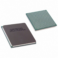
EP1S10F780I6N Altera, EP1S10F780I6N Datasheet - Page 410

EP1S10F780I6N
Manufacturer Part Number
EP1S10F780I6N
Description
IC STRATIX FPGA 10K LE 780-FBGA
Manufacturer
Altera
Series
Stratix®r
Datasheet
1.EP1S10F484I6N.pdf
(864 pages)
Specifications of EP1S10F780I6N
Number Of Logic Elements/cells
10570
Number Of Labs/clbs
1057
Total Ram Bits
920448
Number Of I /o
426
Voltage - Supply
1.425 V ~ 1.575 V
Mounting Type
Surface Mount
Operating Temperature
0°C ~ 85°C
Package / Case
780-FBGA
Lead Free Status / RoHS Status
Lead free / RoHS Compliant
Number Of Gates
-
Available stocks
Company
Part Number
Manufacturer
Quantity
Price
Company:
Part Number:
EP1S10F780I6N
Manufacturer:
ALTERA
Quantity:
3 000
- Current page: 410 of 864
- Download datasheet (11Mb)
DDR Memory Support Overview
3–14
Stratix Device Handbook, Volume 2
The DQS pins are marked in the Stratix and Stratix GX device pin table as
DQS[9..0]T or DQS[9..0]B, where T stands for top and B for bottom.
The corresponding DQ pins are marked as DQ[9..0]T[7..0], where
[9..0] indicates which DQS group the pins belong to. The numbering
scheme starts from right to left on the package bottom view. When not
used as DQ or DQS pins, these pins are available as user I/O pins.
You can also create a design in a mode other than the ×8, ×16, or ×32
mode. The Quartus
unused DQ pins available as regular use I/O pins. For example, if you
create a design for ×9 mode for an RLDRAM II interface (nine DQ pins
driven by one DQS pin), the Quartus II software implements a ×16 mode
with seven DQ pins unconnected to the DQS bus. These seven unused
DQ pins can be used as regular I/O pins.
1
Stratix and Stratix GX device side I/O banks (I/O banks 1, 2, 5, and 6)
support SDR SDRAM, ZBT SRAM, QDR SRAM, QDRII SRAM, and DDR
SDRAM interfaces and can use any of the user I/O pins in these banks for
the interface. Since these I/O banks do not have any dedicated circuitry
for memory interfacing, they can support DDR SDRAM up to 150 MHz
in -5 speed grade devices. However, these I/O banks do not support the
HSTL-18 Class II I/O standard, which is required to interface with
RLDRAM II.
Clock Pins
You can use any of the DDR I/O registers in the top or bottom bank of the
device (I/O banks 3, 4, 7, or 8) to generate clocks to the memory device.
You can also use any of the DDR I/O registers in the side I/O banks 1, 2,
5, or 6 to generate clocks for DDR SDRAM interfaces on the side I/O
banks (not using the DQS circuitry).
On the top and bottom side of the device, the DQ and DQS pins
must be configured as bidirectional DDR pins to enable the DQS
phase-shift circuitry. If you only want to use the DQ and/or
DQS pins as inputs, you need to set the output enable of the DQ
and/or DQS pins to ground. Use the altdqs and altdq
megafunctions to configure the DQS and DQ pins, respectively.
However, you should use the Altera
data path for your memory interfaces.
®
II software uses the next larger mode with the
®
IP Toolbench to create the
Altera Corporation
June 2006
Related parts for EP1S10F780I6N
Image
Part Number
Description
Manufacturer
Datasheet
Request
R

Part Number:
Description:
CYCLONE II STARTER KIT EP2C20N
Manufacturer:
Altera
Datasheet:

Part Number:
Description:
CPLD, EP610 Family, ECMOS Process, 300 Gates, 16 Macro Cells, 16 Reg., 16 User I/Os, 5V Supply, 35 Speed Grade, 24DIP
Manufacturer:
Altera Corporation
Datasheet:

Part Number:
Description:
CPLD, EP610 Family, ECMOS Process, 300 Gates, 16 Macro Cells, 16 Reg., 16 User I/Os, 5V Supply, 15 Speed Grade, 24DIP
Manufacturer:
Altera Corporation
Datasheet:

Part Number:
Description:
Manufacturer:
Altera Corporation
Datasheet:

Part Number:
Description:
CPLD, EP610 Family, ECMOS Process, 300 Gates, 16 Macro Cells, 16 Reg., 16 User I/Os, 5V Supply, 30 Speed Grade, 24DIP
Manufacturer:
Altera Corporation
Datasheet:

Part Number:
Description:
High-performance, low-power erasable programmable logic devices with 8 macrocells, 10ns
Manufacturer:
Altera Corporation
Datasheet:

Part Number:
Description:
High-performance, low-power erasable programmable logic devices with 8 macrocells, 7ns
Manufacturer:
Altera Corporation
Datasheet:

Part Number:
Description:
Classic EPLD
Manufacturer:
Altera Corporation
Datasheet:

Part Number:
Description:
High-performance, low-power erasable programmable logic devices with 8 macrocells, 10ns
Manufacturer:
Altera Corporation
Datasheet:

Part Number:
Description:
Manufacturer:
Altera Corporation
Datasheet:

Part Number:
Description:
Manufacturer:
Altera Corporation
Datasheet:

Part Number:
Description:
Manufacturer:
Altera Corporation
Datasheet:

Part Number:
Description:
CPLD, EP610 Family, ECMOS Process, 300 Gates, 16 Macro Cells, 16 Reg., 16 User I/Os, 5V Supply, 25 Speed Grade, 24DIP
Manufacturer:
Altera Corporation
Datasheet:


