ADSP-3PARCBF548M01 Analog Devices Inc, ADSP-3PARCBF548M01 Datasheet - Page 35
ADSP-3PARCBF548M01
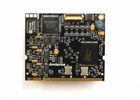
Manufacturer Part Number
ADSP-3PARCBF548M01
Description
MODULE BOARD BF548
Manufacturer
Analog Devices Inc
Series
Blackfin®r
Specifications of ADSP-3PARCBF548M01
Module/board Type
Processor Module
For Use With/related Products
ADSP-BF548
Lead Free Status / RoHS Status
Lead free / RoHS Compliant


7
8
9
10
11
12
13
14
Table 13
ments for the ADSP-BF54x Blackfin processors’ clocks. Take
care in selecting MSEL, SSEL, and CSEL ratios so as not to
exceed the maximum core clock and system clock.
describes the phase-locked loop operating conditions.
Table 13. Core Clock Requirements—533 MHz and 600 MHz Speed Grade
1
2
Table 14. Core Clock Requirements—400 MHz Speed Grade
1
2
Table 15. Phase-Locked Loop Operating Conditions
Table 16. System Clock Requirements
1
2
3
4
Parameter value applies to pins DQ0–15 and DQS0–1.
PB1-0, PE15-14, PG15-11, and PH7-6 are 5.0 V-tolerant (always accept up to 5.5 V maximum V
SDA and SCL are 5.0V tolerant (always accept up to 5.5V maximum V
Parameter
f
f
f
f
f
f
See the
Use of an internal voltage regulator is not supported on automotive grade and 600 MHz speed grade models
Parameter
f
f
f
f
See
Use of an internal voltage regulator is not supported on automotive grade models
Parameter
f
Parameter
f
f
f
Rounded number. Actual test specification is SCLK period of 7.5 ns. See
Rounded number. Actual test specification is SCLK period of 8.33 ns.
V
Parameter value applies to USB_DP, USB_DM, and USB_VBUS pins. See
Parameter value applies to all input and bidirectional pins, except PB1-0, PE15-14, PG15–11, and PH7-6.
Parameter value applies to pins PG15–11 and PH7-6.
Parameter value applies to pins PB1-0 and PE15-14. Consult the I
T
CCLK
CCLK
CCLK
CCLK
CCLK
CCLK
CCLK
CCLK
CCLK
CCLK
VCO
SCLK
SCLK
SCLK
V
DDINT
J
OH
must be in the range: 0°C < T
Ordering Guide on Page 100
) is limited by V
must be less than or equal to f
must be greater than or equal to 1.14 V for mobile DDR SDRAM models. See
Ordering Guide on Page
and
Table 16
Condition
V
V
Core Clock Frequency
Core Clock Frequency
Core Clock Frequency
Core Clock Frequency
Core Clock Frequency
Core Clock Frequency
Core Clock Frequency
Core Clock Frequency
Core Clock Frequency
Core Clock Frequency
DDINT
DDINT
DDEXT
Voltage Controlled Oscillator (VCO) Frequency
≥ 1.14 V
< 1.14 V
supply voltage.
describe the voltage/frequency require-
ADSP-BF542/ADSP-BF544/ADSP-BF547/ADSP-BF548/ADSP-BF549
J
100.
< 55°C during OTP memory programming operations.
CCLK
1
1
.
Condition
V
V
V
V
V
V
V
V
Condition
V
V
DDINT
DDINT
DDINT
DDINT
DDINT
DDINT
DDINT
DDINT
DDINT
DDINT
= 1.30 V minimum
= 1.20 V minimum
= 1.14 V minimum
= 1.045 V minimum
= 0.95 V minimum
= 0.90 Vminimum
= 1.14 V minimum
= 1.045 V minimum
= 0.95 V minimum
= 0.90 V minimum
Rev. C | Page 35 of 100 | February 2010
Table 15
2
C specification version 2.1 for the proper resistor value and other open drain pin electrical parameters.
IH
). Voltage compliance on outputs (V
Table 26 on Page
Absolute Maximum Ratings on Page
DDR SDRAM Models Mobile DDR SDRAM Models
Max
133
100
1
2
Operating Conditions on Page
Internal Regulator Setting
N/A
1.20 V
1.25 V
1.10 V
1.00 V
0.95 V
43.
Internal Regulator Setting
1.20 V
1.10 V
1.00 V
0.95 V
2
IH
1
when power is applied to V
Min
120
N/A
OH
3
4
) is limited by the
40.
Min
50
34.
2
DDEXT
2
Max
133
N/A
VDDEXT
Max
600
533
500
444
400
333
400
364
333
300
Max
pins). Voltage compliance (on output
2
4
Max
Maximum f
supply voltage.
Unit
MHz
MHz
MHz
MHz
CCLK
Unit
MHz
MHz
Unit
MHz
MHz
MHz
MHz
MHz
MHz
Unit
MHz
Related parts for ADSP-3PARCBF548M01
Image
Part Number
Description
Manufacturer
Datasheet
Request
R

Part Number:
Description:
±1.7g Dual-Axis IMEMS Accelerometer Evaluation Board
Manufacturer:
Analog Devices Inc
Datasheet:

Part Number:
Description:
Inertial Sensor Evaluation System
Manufacturer:
Analog Devices Inc
Datasheet:
Part Number:
Description:
Manufacturer:
Analog Devices Inc
Datasheet:
Part Number:
Description:
Manufacturer:
Analog Devices Inc
Datasheet:
Part Number:
Description:
Manufacturer:
Analog Devices Inc
Datasheet:
Part Number:
Description:
Manufacturer:
Analog Devices Inc
Datasheet:
Part Number:
Description:
Manufacturer:
Analog Devices Inc
Datasheet:
Part Number:
Description:
Manufacturer:
Analog Devices Inc
Datasheet:
Part Number:
Description:
Manufacturer:
Analog Devices Inc
Datasheet:
Part Number:
Description:
Manufacturer:
Analog Devices Inc
Datasheet:
Part Number:
Description:
Manufacturer:
Analog Devices Inc
Datasheet:
Part Number:
Description:
Manufacturer:
Analog Devices Inc
Datasheet:
Part Number:
Description:
Manufacturer:
Analog Devices Inc
Datasheet: