ADSP-3PARCBF548M01 Analog Devices Inc, ADSP-3PARCBF548M01 Datasheet - Page 67
ADSP-3PARCBF548M01
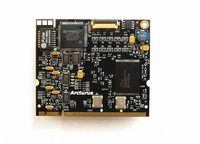
Manufacturer Part Number
ADSP-3PARCBF548M01
Description
MODULE BOARD BF548
Manufacturer
Analog Devices Inc
Series
Blackfin®r
Specifications of ADSP-3PARCBF548M01
Module/board Type
Processor Module
For Use With/related Products
ADSP-BF548
Lead Free Status / RoHS Status
Lead free / RoHS Compliant


Timer Cycle Timing
Table 48
input signal is asynchronous in “width capture mode” and
“external clock mode” and has an absolute maximum input fre-
quency of (f
Table 48. Timer Cycle Timing
1
2
Parameter
Timing Characteristics
t
t
t
t
Switching Characteristics
t
t
The minimum pulse widths apply for TMRx signals in width capture and external clock modes.
Either a valid setup and hold time or a valid pulse width is sufficient. There is no need to resynchronize timer flag inputs.
WL
WH
TIS
TIH
HTO
TOD
and
SCLK
Figure 41
/2) MHz.
TMRx OUTPUT
TMRx INPUT
Timer Pulse Width Input Low
Timer Pulse Width Input High
Timer Input Setup Time Before CLKOUT Low
Timer Input Hold Time After CLKOUT Low
Timer Pulse Width Output
Timer Output Delay After CLKOUT High
CLKOUT
describe timer expired operations. The
ADSP-BF542/ADSP-BF544/ADSP-BF547/ADSP-BF548/ADSP-BF549
1
1
Rev. C | Page 67 of 100 | February 2010
t
TIS
Figure 41. Timer Cycle Timing
2
t
2
WH
,t
WL
t
TIH
t
TOD
t
HTO
Min
t
t
6.5
–1
1×t
SCLK
SCLK
SCLK
+1
+1
Max
(2
6
32
– 1)×t
SCLK
Unit
ns
ns
ns
ns
ns
ns
Related parts for ADSP-3PARCBF548M01
Image
Part Number
Description
Manufacturer
Datasheet
Request
R

Part Number:
Description:
±1.7g Dual-Axis IMEMS Accelerometer Evaluation Board
Manufacturer:
Analog Devices Inc
Datasheet:

Part Number:
Description:
Inertial Sensor Evaluation System
Manufacturer:
Analog Devices Inc
Datasheet:
Part Number:
Description:
Manufacturer:
Analog Devices Inc
Datasheet:
Part Number:
Description:
Manufacturer:
Analog Devices Inc
Datasheet:
Part Number:
Description:
Manufacturer:
Analog Devices Inc
Datasheet:
Part Number:
Description:
Manufacturer:
Analog Devices Inc
Datasheet:
Part Number:
Description:
Manufacturer:
Analog Devices Inc
Datasheet:
Part Number:
Description:
Manufacturer:
Analog Devices Inc
Datasheet:
Part Number:
Description:
Manufacturer:
Analog Devices Inc
Datasheet:
Part Number:
Description:
Manufacturer:
Analog Devices Inc
Datasheet:
Part Number:
Description:
Manufacturer:
Analog Devices Inc
Datasheet:
Part Number:
Description:
Manufacturer:
Analog Devices Inc
Datasheet:
Part Number:
Description:
Manufacturer:
Analog Devices Inc
Datasheet: