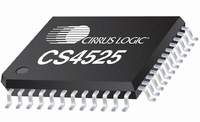
CS4525-CNZ Cirrus Logic Inc, CS4525-CNZ Datasheet - Page 63

CS4525-CNZ
Manufacturer Part Number
CS4525-CNZ
Description
IC AMP AUDIO PWR 30W QUAD 48QFN
Manufacturer
Cirrus Logic Inc
Series
Popguard®r
Type
Class Dr
Datasheet
1.CS4525-CNZ.pdf
(98 pages)
Specifications of CS4525-CNZ
Output Type
2-Channel (Stereo) or 4-Channel (Quad)
Package / Case
48-QFN
Max Output Power X Channels @ Load
30W x 1 @ 4 Ohm; 15W x 2 @ 8 Ohm
Voltage - Supply
8 V ~ 18 V
Features
ADC, Depop, I²C, I²S, Mute, PWM, Short-Circuit and Thermal Protection, Volume Control
Mounting Type
Surface Mount
Product
Class-D
Output Power
30 W
Thd Plus Noise
10 %
Operating Supply Voltage
2.5 V to 5 V
Supply Current
54 mA
Maximum Power Dissipation
180 mW
Maximum Operating Temperature
+ 70 C
Mounting Style
SMD/SMT
Audio - Load Impedance
4 Ohms, 6 Ohms, 8 Ohms
Audio Load Resistance
8 Ohms, 4 Ohms
Minimum Operating Temperature
0 C
Supply Voltage (max)
5.25 V
Supply Voltage (min)
2.375 V
Amplifier Class
D
No. Of Channels
4
Supply Voltage Range
8V To 18V
Load Impedance
4ohm
Operating Temperature Range
0°C To +70°C
Amplifier Case Style
QFN
No. Of Pins
48
Rohs Compliant
Yes
Lead Free Status / RoHS Status
Lead free / RoHS Compliant
For Use With
598-1586 - REFERENCE BOARD FOR CS4525 PWM
Lead Free Status / Rohs Status
Lead free / RoHS Compliant
Other names
598-1264
Available stocks
Company
Part Number
Manufacturer
Quantity
Price
Company:
Part Number:
CS4525-CNZ
Manufacturer:
CRYSTAL
Quantity:
329
Part Number:
CS4525-CNZ
Manufacturer:
TI/德州仪器
Quantity:
20 000
Part Number:
CS4525-CNZR
Manufacturer:
CIRRUSLOGICINC
Quantity:
20 000
DS726PP2
6.6.3
6.7
Integrated VD Regulator
The CS4525 includes two internal linear regulators, one from the VD supply voltage to provide a fixed
supply to its internal digital blocks, and another from the VD supply voltage to provide a fixed
to its internal analog blocks. The LVD pin must be set to indicate the voltage present on the VD pin as shown
in
The output of the digital regulator is presented on the VD_REG pin and may be used to provide an external
device with up to
is presented on the VA_REG pin and must only be connected to the bypass capacitors as shown in the typ-
ical connection diagrams.
If a nominal supply voltage of 2.5 V is used as the VD supply (see the
table on
this configuration, the internal regulators are bypassed and the external supply source is used to directly
drive the internal digital and analog sections.
Referenced Control
SelectVD .............................
Right-Justified Data Format
In Right-Justified format, data is received most significant bit first and with the least significant bit present-
ed on the last SCLK before the LRCK transition and is valid on the rising edge of SCLK. For the Right-
Justified format, the left channel data is presented when LRCK is high and the right channel data is pre-
sented when LRCK is low. 16, 18, 20, and 24 bits per sample are supported.
Table 21
3.3 V Supply
2.5 V Supply
Connection
5 V Supply
SCLK
LRCK
SDIN
VD
page
below.
18), the VD, VD_REG, and VA_REG pins must all be connected to the VD supply source. In
3 mA
VD and Bypass Capacitors
Bypass Capacitors Only
Bypass Capacitors Only
Register Location
“Select VD Level (SelectVD)” on page 88
of current at its nominal output voltage of
Connection
15 14 13 12 11 10
VD_REG
Table 21. Power Supply Configuration and Settings
Figure 32. Right-Justified Serial Audio Formats
Left Channel
9 8 7
VD and Bypass Capacitors
6 5 4 3 2 1 0
Bypass Capacitors Only
Bypass Capacitors Only
Connection
VA_REG
2.5
V. The output of the analog regulator
Recommended Operating Conditions
15 14 13 12 11 10
Connection
DGND
DGND
LVD
VD
Right Channel
9 8 7
SelectVD Bit Setting
Software Mode Only
6 5 4 3 2 1 0
‘1’ - Default
‘1’ - Default
‘0’
2.5 V
CS4525
supply
2.5 V
63


