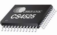
CS4525-CNZ Cirrus Logic Inc, CS4525-CNZ Datasheet - Page 73

CS4525-CNZ
Manufacturer Part Number
CS4525-CNZ
Description
IC AMP AUDIO PWR 30W QUAD 48QFN
Manufacturer
Cirrus Logic Inc
Series
Popguard®r
Type
Class Dr
Datasheet
1.CS4525-CNZ.pdf
(98 pages)
Specifications of CS4525-CNZ
Output Type
2-Channel (Stereo) or 4-Channel (Quad)
Package / Case
48-QFN
Max Output Power X Channels @ Load
30W x 1 @ 4 Ohm; 15W x 2 @ 8 Ohm
Voltage - Supply
8 V ~ 18 V
Features
ADC, Depop, I²C, I²S, Mute, PWM, Short-Circuit and Thermal Protection, Volume Control
Mounting Type
Surface Mount
Product
Class-D
Output Power
30 W
Thd Plus Noise
10 %
Operating Supply Voltage
2.5 V to 5 V
Supply Current
54 mA
Maximum Power Dissipation
180 mW
Maximum Operating Temperature
+ 70 C
Mounting Style
SMD/SMT
Audio - Load Impedance
4 Ohms, 6 Ohms, 8 Ohms
Audio Load Resistance
8 Ohms, 4 Ohms
Minimum Operating Temperature
0 C
Supply Voltage (max)
5.25 V
Supply Voltage (min)
2.375 V
Amplifier Class
D
No. Of Channels
4
Supply Voltage Range
8V To 18V
Load Impedance
4ohm
Operating Temperature Range
0°C To +70°C
Amplifier Case Style
QFN
No. Of Pins
48
Rohs Compliant
Yes
Lead Free Status / RoHS Status
Lead free / RoHS Compliant
For Use With
598-1586 - REFERENCE BOARD FOR CS4525 PWM
Lead Free Status / Rohs Status
Lead free / RoHS Compliant
Other names
598-1264
Available stocks
Company
Part Number
Manufacturer
Quantity
Price
Company:
Part Number:
CS4525-CNZ
Manufacturer:
CRYSTAL
Quantity:
329
Part Number:
CS4525-CNZ
Manufacturer:
TI/德州仪器
Quantity:
20 000
Part Number:
CS4525-CNZR
Manufacturer:
CIRRUSLOGICINC
Quantity:
20 000
DS726PP2
9.3.5
9.4
9.4.1
9.4.2
9.4.3
OutputCfg1
7
Output Configuration (Address 04h)
Aux Serial Port Left Channel Data Select (LChDSel[1:0])
Default = 00
Function:
Selects the data to be sent over the left channel of the auxiliary port serial data output signal.
Output Configuration (OutputCfg[1:0])
Default = 00
Function:
Identifies the power output configuration. This parameter can only be changed when all modulators and
associated logic are in the power-down state (the PDnAll bit is set). Attempts to write this register while
the PDnAll is cleared will be ignored. See
tion.
PWM Signals Output Data Select (PWMDSel[1:0])
Default = 00
Function:
Selects the PWM data output on the PWM_SIG1 and PWM_SIG2 output signals.See
Level Output Configurations” on page 49
Channel Delay Settings (OutputDly[3:0])
Default = 0000
Function:
The channel delay bits allow delay adjustment of each of the power output audio channels. The value of
this register determines the amount of delay inserted in the output path. The delay time is calculated by
multiplying the register value by the period of the SYS_CLK or crystal input clock source. These bits can
LChDSel[1:0] Setting
OutputCfg[1:0] Setting
PWMDSel Setting
00 ........................................Channel A.
01 ........................................Channel B.
10 ........................................Sub Channel.
11.........................................Channel B crossover low-pass output.
00 ........................................Channel 1 & 2 Full-Bridge.
01 ........................................Channel 1 & 2 Half-Bridge + Sub Channel Full-Bridge.
10 ........................................Channel 1 Parallel Full-Bridge.
11.........................................Reserved.
00 ........................................PWM_SIG1 output disabled.
01 ........................................Channel 1 output on PWM_SIG1.
10 ........................................Channel 1 output on PWM_SIG1.
11.........................................Channel 2 output on PWM_SIG1.
OutputCfg0
6
PWMDSel1
Aux Serial Port Left Channel Output Data Source
Power Output Configuration
PWM Signal Output Mapping
PWM_SIG2 output disabled.
Channel 2 output on PWM_SIG2.
Sub Channel output on PWM_SIG2.
Sub Channel output on PWM_SIG2.
5
PWMDSel0
4
for more information.
“Output Channel Configurations” on page 45
OutputDly3
3
OutputDly2
2
OutputDly1
1
“PWM_SIG Logic-
for more informa-
OutputDly0
CS4525
0
73


