KDC5612EVAL Intersil, KDC5612EVAL Datasheet
KDC5612EVAL
Specifications of KDC5612EVAL


Related parts for KDC5612EVAL

KDC5612EVAL Summary of contents
Page 1
... KAD5610P-17 KAD5610P-12 CAUTION: These devices are sensitive to electrostatic discharge; follow proper IC Handling Procedures. 1-888-INTERSIL or 1-888-468-3774 FemtoCharge is a trademark of Kenet Inc. Copyright Intersil Americas Inc. 2008, 2009. All Rights Reserved All other trademarks mentioned are the property of their respective owners. KAD5612P FN6803.2 ...
Page 2
... These Intersil Pb-free plastic packaged products employ special Pb-free material sets; molding compounds/die attach materials and NiPdAu plate - e4 termination finish, which is RoHS compliant and compatible with both SnPb and Pb-free soldering operations. Intersil Pb-free products are MSL classified at Pb-free peak reflow temperatures that meet or exceed the Pb-free requirements of IPC/JEDEC J STD-020. ...
Page 3
Table of Contents Absolute Maximum Ratings ......................................... 4 Thermal Information...................................................... 4 Electrical Specifications ............................................... 4 Digital Specifications .................................................... 6 Timing Diagrams ........................................................... 7 Switching Specifications .............................................. 7 Pinout/Package Information......................................... 8 Pin Descriptions.......................................................... 8 Pinout ......................................................................... 10 Typical Performance Curves ........................................ ...
Page 4
... D 4 KAD5612P Thermal Information Thermal Resistance (Typical, Note QFN . . . . . . . . . . . . . . . . . . . . . . . . . . . . . . . . Operating Temperature . . . . . . . . . . . . . . . . . . . . . . .-40°C to +85°C Storage Temperature . . . . . . . . . . . . . . . . . . . . . . . .-65°C to +150°C Junction Temperature . . . . . . . . . . . . . . . . . . . . . . . . . . . . . . +150°C Pb-Free Reflow Profile .see link below http://www.intersil.com/pbfree/Pb-FreeReflow.asp = -1dBFS KAD5612P-25 KAD5612P-21 (Note 3) (Note 3) MIN TYP MAX MIN TYP MAX MIN 1 ...
Page 5
Electrical Specifications All specifications apply under the following conditions unless otherwise noted: AVDD = 1.8V, OVDD = 1.8V -40°C to +85°C (typical specifications at +25°C (per speed grade). (Continued) PARAMETER SYMBOL CONDITIONS Nap Mode P D ...
Page 6
Electrical Specifications All specifications apply under the following conditions unless otherwise noted: AVDD = 1.8V, OVDD = 1.8V -40°C to +85°C (typical specifications at +25°C (per speed grade). (Continued) PARAMETER SYMBOL CONDITIONS Intermodulation IMD f = ...
Page 7
Timing Diagrams SAMPLE N INP INN t A CLKN CLKP t LATENCY = L CYCLES CPD CLKOUTN CLKOUTP D[11:0]P A DATA B DATA A DATA B DATA A DATA N-L N-L N N-L + ...
Page 8
Pinout/Package Information Pin Descriptions PIN NUMBER LVDS [LVCMOS] NAME 1, 6, 19, 24, 71 AVDD 2-5, 17, 18, 28-31 DNC 7, 10-12, 72 AVSS 8, 9 BINP, BINN 13, 14 AINN, AINP 15 VCM 16 CLKDIV 20, 21 CLKP, CLKN ...
Page 9
Pin Descriptions (Continued) PIN NUMBER LVDS [LVCMOS] NAME 50 D6P [D6] 51 D7N [NC] 52 D7P [D7] 53 D8N [NC] 54 D8P [D8] 57 D9N [NC] 58 D9P [D9] 59 D10N [NC] 60 D10P [D10] 61 D11N [NC] 62 D11P ...
Page 10
Pinout AVDD 1 DNC 2 3 DNC 4 DNC 5 DNC 6 AVDD 7 AVSS 8 BINP 9 BINN 10 AVSS 11 AVSS 12 AVSS 13 AINN 14 AINP 15 VCM 16 CLKDIV 17 DNC DNC 18 ...
Page 11
Typical Performance Curves 90 85 SFDR @ 125MSPS 80 75 SNR @ 125MSPS SNR @ 250MSPS 55 SFDR @ 250MSPS 50 0 200M 400M INPUT FREQUENCY (Hz) FIGURE 4. SNR AND SFDR vs f 100 90 80 ...
Page 12
Typical Performance Curves 500 450 400 350 300 250 200 150 100 100 130 SAMPLE RATE (MSPS) FIGURE 10. POWER vs f SAMPLE 1.5 1.0 0.5 0 -0.5 -1.0 -1.5 0 512 1024 1536 2048 CODE ...
Page 13
Typical Performance Curves 0 AIN = -1.0dBFS SNR = 66.0dBFS -20 SFDR = 86.5dBc SINAD = 65.9dBFS -40 -60 -80 -100 -120 0M 20M 40M 60M FREQUENCY (Hz) FIGURE 16. SINGLE-TONE SPECTRUM @ 105MHz 0 AIN = -1.0dBFS SNR = ...
Page 14
Theory of Operation Functional Description The KAD5612P is based upon a 12-bit, 250MSPS A/D converter core that utilizes a pipelined successive approximation architecture (Figure 22). The input voltage is captured by a Sample-Hold Amplifier (SHA) and converted to a unit ...
Page 15
The calibration sequence is initiated on the rising edge of RESETN, as shown in Figure 23. The over-range output (OR) is set high once RESETN is pulled low, and remains in that state until calibration is complete. The OR output ...
Page 16
INP 1.0 0.725V 0.6 0.2 FIGURE 26. ANALOG INPUT RANGE An RF transformer will give the best noise and distortion performance for wideband and/or high intermediate frequency (IF) inputs. Two different transformer input schemes are shown in Figures ...
Page 17
A delay-locked loop (DLL) generates internal clock signals for various stages within the charge pipeline. If the frequency of the input clock changes, the DLL may take up to 52µs to regain lock at 250MSPS. The lock time is inversely ...
Page 18
Wake-up from Sleep Mode Sequence (CSB high) • Pull CSB Low • Wait 150us • Write ‘001x’ to Register 25 • Wait 1ms until ADC fully powered application where CSB was kept low in sleep mode, the ...
Page 19
CSB SCLK SDIO R CSB SCLK SDIO Serial Peripheral Interface A serial peripheral interface (SPI) bus is used to facilitate configuration of the device and to optimize performance. The SPI bus consists of chip select ...
Page 20
DSW CSB t S SCLK SDIO R A12 t DSW t DHW t CSB S SCLK SDIO R A12 SDO CSB SCLK SDIO INSTRUCTION/ADDRESS CSB SCLK SDIO INSTRUCTION/ADDRESS 20 KAD5612P t t CLK HI t ...
Page 21
... KAD5612P Indexed Device Configuration/Control ADDRESS 0X10: DEVICE_INDEX_A 1 A common SPI map, which can accommodate single-channel or multi-channel devices, is used for all Intersil ADC products. 2 Certain configuration commands (identified as Indexed in the 3 SPI map) can be executed on a per-converter basis. This 4 or more register determines which converter is being addressed for an Indexed command ...
Page 22
TABLE 8. COARSE GAIN ADJUSTMENT NOMINAL COARSE GAIN ADJUST 0x22[3:0] Bit3 Bit2 Bit1 Bit0 TABLE 9. MEDIUM AND FINE GAIN ADJUSTMENTS 0x23[7:0] PARAMETER MEDIUM GAIN Steps 256 –Full Scale (0x00) -2% Mid–Scale (0x80) 0.00% +Full Scale (0xFF) +2% Nominal Step ...
Page 23
OUTFMT pin selects the data format (refer to “Data Format” on page 18). This functionality can be overridden and controlled through the SPI, as shown in Table 14. This register is not changed by a Soft Reset. TABLE 13. ...
Page 24
SPI Memory Map ADDR PARAMETER BIT 7 (Hex) NAME (MSB) 00 port_config SDO LSB First Active 01 reserved 02 burst_end 03-07 reserved 08 chip_id 09 chip_version 10 device_index_A 11-1F reserved 20 offset_coarse 21 offset_fine 22 gain_coarse 23 gain_medium 24 gain_fine ...
Page 25
ADDR PARAMETER BIT 7 (Hex) NAME (MSB) C0 test_io User Test Mode [1: Single 01 = Alternate 10 = Reserved 11 = Reserved C1 Reserved C2 user_patt1_lsb B7 C3 user_patt1_msb B15 C4 user_patt2_lsb B7 C5 user_patt2_msb B15 C6-FF ...
Page 26
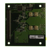
... FIGURE 46. LVDS OUTPUTS 0.535V ADC Evaluation Platform Intersil offers an ADC Evaluation platform which can be used to evaluate any of the KADxxxxx ADC family. The platform consists of a FPGA based data capture motherboard and a family of ADC daughter cards. This USB based platform allows a user to quickly evaluate the ADC’s performance at a user’ ...
Page 27
LVDS Outputs Output traces and connections must be designed for 50Ω (100Ω differential) characteristic impedance. Keep traces direct and minimize bends where possible. Avoid crossing ground and power-plane breaks with signal traces. LVCMOS Outputs Output traces and connections must be ...
Page 28
... Accordingly, the reader is cautioned to verify that data sheets are current before placing orders. Information furnished by Intersil is believed to be accurate and reliable. However, no responsibility is assumed by Intersil or its subsidiaries for its use; nor for any infringements of patents or other rights of third parties which may result from its use ...
Page 29
Package Outline Drawing L72.10x10D 72 LEAD QUAD FLAT NO-LEAD PLASTIC PACKAGE Rev 1, 11/08 10.00 PIN 1 INDEX AREA 6 (4X) 0.15 TOP VIEW 9.80 Sq 6.00 Sq TYPICAL RECOMMENDED LAND PATTERN 29 KAD5612P 10.00 37 ...