KDC5612EVAL Intersil, KDC5612EVAL Datasheet - Page 22
KDC5612EVAL
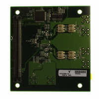
Manufacturer Part Number
KDC5612EVAL
Description
DAUGHTER CARD FOR KAD5612
Manufacturer
Intersil
Series
FemtoCharge™r
Datasheets
1.KAD5612P-25Q72.pdf
(29 pages)
2.KMB-001LEVALZ.pdf
(7 pages)
3.KDC5514EVALZ.pdf
(9 pages)
Specifications of KDC5612EVAL
Number Of Adc's
2
Number Of Bits
12
Sampling Rate (per Second)
250M
Data Interface
Parallel
Inputs Per Adc
1 Differential
Input Range
1.47 Vpp
Power (typ) @ Conditions
429mW @ 250MSPS
Voltage Supply Source
Single Supply
Operating Temperature
-40°C ~ 85°C
Utilized Ic / Part
KAD5612P-25, KMB001 Motherboard
For Use With
KMB001LEVAL - MOTHERBOARD FOR LVDS ADC CARD
Lead Free Status / RoHS Status
Lead free / RoHS Compliant


ADDRESS 0X25: MODES
Two distinct reduced power modes can be selected. By
default, the tri-level NAPSLP pin can select normal
operation, nap or sleep modes (refer to “Nap/Sleep” on
page 17). This functionality can be overridden and controlled
through the SPI. This is an indexed function when controlled
from the SPI, but a global function when driven from the pin.
This register is not changed by a Soft Reset.
Global Device Configuration/Control
ADDRESS 0X70: SKEW_DIFF
The value in the skew_diff register adjusts the timing skew
between the two ADCs cores. The nominal range and
resolution of this adjustment are given in Table 11. The
default value of this register after power-up is 00h.
+Full Scale (0xFF)
Nominal Step Size
–Full Scale (0x00)
Mid–Scale (0x80)
PARAMETER
TABLE 9. MEDIUM AND FINE GAIN ADJUSTMENTS
+Full Scale (0xFF)
–Full Scale (0x00)
Nominal Step Size
TABLE 11. DIFFERENTIAL SKEW ADJUSTMENT
Mid–Scale (0x80)
0x22[3:0]
Steps
PARAMETER
Bit3
Bit2
Bit1
Bit0
TABLE 8. COARSE GAIN ADJUSTMENT
VALUE
TABLE 10. POWER DOWN CONTROL
Steps
000
001
010
100
MEDIUM GAIN
NOMINAL COARSE GAIN ADJUST
0x23[7:0]
0.016%
0.00%
+2%
-2%
256
22
POWER-DOWN MODE
DIFFERENTIAL SKEW
Normal Operation
Sleep Mode
+2.8
+1.4
-2.8
-1.4
Pin Control
(%)
Nap Mode
0x25[2:0]
0x70[7:0]
+6.5ps
-6.5ps
0.0ps
51fs
256
FINE GAIN
0x24[7:0]
0.0016%
-0.20%
0.00%
+0.2%
256
KAD5612P
SLIP TWICE
SLIP ONCE
ADDRESS 0X71: PHASE_SLIP
When using the clock divider, it’s not possible to determine the
synchronization of the incoming and divided clock phases.
This is particularly important when multiple ADCs are used in
a time-interleaved system. The phase slip feature allows the
rising edge of the divided clock to be advanced by one input
clock cycle when in CLK/4 mode, as shown in Figure 40.
Execution of a phase_slip command is accomplished by first
writing a ‘0’ to bit 0 at address 71h followed by writing a ‘1’ to
bit 0 at address 71h (32 sclk cycles).
ADDRESS 0X72: CLOCK_DIVIDE
The KAD5612P has a selectable clock divider that can be
set to divide by four, two or one (no division). By default, the
tri-level CLKDIV pin selects the divisor (refer to “Clock Input”
on page 16). This functionality can be overridden and
controlled through the SPI, as shown in Table 12. This
register is not changed by a Soft Reset.
ADDRESS 0X73: OUTPUT_MODE_A
The output_mode_A register controls the physical output
format of the data, as well as the logical coding. The
KAD5612P can present output data in two physical formats:
LVDS or LVCMOS. Additionally, the drive strength in LVDS
mode can be set high (3mA) or low (2mA). By default, the
tri-level OUTMODE pin selects the mode and drive level
(refer to “Digital Outputs” on page 17). This functionality can
be overridden and controlled through the SPI, as shown in
Table 13.
Data can be coded in three possible formats: two’s
complement, Gray code or offset binary. By default, the
FIGURE 40. PHASE SLIP: CLK ÷ 4 MODE, f
CLK
CLK
CLK
CLK
÷ 4
÷ 4
÷ 4
TABLE 12. CLOCK DIVIDER SELECTION
VALUE
000
001
010
100
CLK = CLKP - CLKN
1.00ns
CLOCK DIVIDER
4.00ns
Pin Control
Divide by 1
Divide by 2
Divide by 4
0x72[2:0]
CLOCK
September 9, 2009
= 1000MHz
FN6803.2
Related parts for KDC5612EVAL
Image
Part Number
Description
Manufacturer
Datasheet
Request
R

Part Number:
Description:
Intersil Corporation [CMOS Serial Controller Interface]
Manufacturer:
Intersil Corporation
Datasheet:
Part Number:
Description:
Manufacturer:
Intersil Corporation
Datasheet:
Part Number:
Description:
357-036-542-201 CARDEDGE 36POS DL .156 BLK LOPRO
Manufacturer:
Intersil Corporation
Datasheet:
Part Number:
Description:
1024-Word x 4-Bit LSI Static RAM
Manufacturer:
Intersil Corporation
Datasheet:
Part Number:
Description:
General Purpose NPN Transistor Arrays FN341.4
Manufacturer:
Intersil Corporation
Datasheet:
Part Number:
Description:
CMOS 16-Bit Microprocessor
Manufacturer:
Intersil Corporation
Datasheet:
Part Number:
Description:
Manufacturer:
Intersil Corporation
Datasheet:
Part Number:
Description:
Manufacturer:
Intersil Corporation
Datasheet:
Part Number:
Description:
Manufacturer:
Intersil Corporation
Datasheet:
Part Number:
Description:
Manufacturer:
Intersil Corporation
Datasheet:
Part Number:
Description:
CMOS 6-Bit Latch and Decoder Memory Interfaces
Manufacturer:
Intersil Corporation
Datasheet:
Part Number:
Description:
CA3046General Purpose NPN Transistor Arrays
Manufacturer:
Intersil Corporation
Datasheet:
Part Number:
Description:
Manufacturer:
Intersil Corporation
Datasheet:
Part Number:
Description:
TR909 DLC/FLC SLIC with Low Power Standby
Manufacturer:
Intersil Corporation
Datasheet:
Part Number:
Description:
Manufacturer:
Intersil Corporation
Datasheet: