KDC5612EVAL Intersil, KDC5612EVAL Datasheet - Page 4
KDC5612EVAL
Manufacturer Part Number
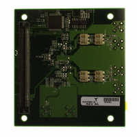
KDC5612EVAL
Description
DAUGHTER CARD FOR KAD5612
Manufacturer
Intersil
Series
FemtoCharge™r
Datasheets
1.KAD5612P-25Q72.pdf
(29 pages)
2.KMB-001LEVALZ.pdf
(7 pages)
3.KDC5514EVALZ.pdf
(9 pages)
Specifications of KDC5612EVAL
Number Of Adc's
2
Number Of Bits
12
Sampling Rate (per Second)
250M
Data Interface
Parallel
Inputs Per Adc
1 Differential
Input Range
1.47 Vpp
Power (typ) @ Conditions
429mW @ 250MSPS
Voltage Supply Source
Single Supply
Operating Temperature
-40°C ~ 85°C
Utilized Ic / Part
KAD5612P-25, KMB001 Motherboard
For Use With
KMB001LEVAL - MOTHERBOARD FOR LVDS ADC CARD
Lead Free Status / RoHS Status
Lead free / RoHS Compliant


Electrical Specifications
Absolute Maximum Ratings
AVDD to AVSS. . . . . . . . . . . . . . . . . . . . . . . . . . . . . . . -0.4V to 2.1V
OVDD to OVSS . . . . . . . . . . . . . . . . . . . . . . . . . . . . . . -0.4V to 2.1V
AVSS to OVSS. . . . . . . . . . . . . . . . . . . . . . . . . . . . . . . -0.3V to 0.3V
Analog Inputs to AVSS. . . . . . . . . . . . . . . . . . -0.4V to AVDD + 0.3V
Clock Inputs to AVSS. . . . . . . . . . . . . . . . . . . -0.4V to AVDD + 0.3V
Logic Input to AVSS . . . . . . . . . . . . . . . . . . . . -0.4V to OVDD + 0.3V
Logic Inputs to OVSS. . . . . . . . . . . . . . . . . . . -0.4V to OVDD + 0.3V
CAUTION: Do not operate at or near the maximum ratings listed for extended periods of time. Exposure to such conditions may adversely impact product reliability and
result in failures not covered by warranty.
NOTE:
DC SPECIFICATIONS
Analog Input
Full-Scale Analog
Input Range
Input Resistance
Input Capacitance
Full Scale Range
Temp. Drift
Input Offset Voltage
Gain Error
Common-Mode
Output Voltage
Clock Inputs
Inputs Common
Mode Voltage
CLKP,CLKN Input
Swing
Power Requirements
1.8V Analog Supply
Voltage
1.8V Digital Supply
Voltage
1.8V Analog Supply
Current
1.8V Digital Supply
Current (Note 4)
Power Supply
Rejection Ratio
Total Power Dissipation
Normal Mode
2. θ
PARAMETER
Tech Brief TB379.
JA
is measured in free air with the component mounted on a high effective thermal conductivity test board with “direct attach” features. See
SYMBOL
OVDD
I
PSRR
AVDD
I
A
OVDD
AVDD
V
V
V
R
C
E
P
VTC
CM
OS
FS
IN
IN
G
D
All specifications apply under the following conditions unless otherwise noted: AVDD = 1.8V, OVDD = 1.8V,
T
(per speed grade).
4
A
Differential
Differential
Differential
Full Temp
3mA LVDS
30MHz, 200mV
signal on AVDD
3mA LVDS
= -40°C to +85°C (typical specifications at +25°C), A
CONDITIONS
P-P
MIN
1.40
435
-10
1.7
1.7
KAD5612P-25
(Note 3)
1000
TYP
1.47
535
170
429
-36
1.8
0.9
1.8
1.8
1.8
90
±2
±2
68
KAD5612P
MAX MIN
1.54 1.40
635
177
456
1.9
1.9
10
76
435
-10
1.7
1.7
Thermal Information
Thermal Resistance (Typical, Note 2)
Operating Temperature . . . . . . . . . . . . . . . . . . . . . . .-40°C to +85°C
Storage Temperature . . . . . . . . . . . . . . . . . . . . . . . .-65°C to +150°C
Junction Temperature . . . . . . . . . . . . . . . . . . . . . . . . . . . . . . +150°C
Pb-Free Reflow Profile. . . . . . . . . . . . . . . . . . . . . . . . .see link below
KAD5612P-21
72 Ld QFN . . . . . . . . . . . . . . . . . . . . . . . . . . . . . . . .
http://www.intersil.com/pbfree/Pb-FreeReflow.asp
(Note 3)
1000
TYP
1.47
535
158
405
-36
1.8
0.9
1.8
1.8
1.8
90
±2
±2
66
IN
MAX MIN
1.54 1.40
635
165
432
1.9
1.9
= -1dBFS, f
10
74
435
-10
1.7
1.7
KAD5612P-17
(Note 3)
SAMPLE
1000
TYP
1.47
535
142
372
1.8
0.9
1.8
1.8
1.8
-36
90
±2
±2
64
MAX MIN
1.54 1.40
635
152
405
= Maximum Conversion Rate
1.9
1.9
10
72
435
-10
1.7
1.7
KAD5612P-12
(Note 3)
1000
1.47
TYP
535
128
342
1.8
0.9
1.8
1.8
1.8
-36
90
±2
±2
62
September 9, 2009
MAX
1.54
635
135
369
1.9
1.9
10
70
θ
JA
ppm/°C
FN6803.2
UNITS
(°C/W)
24
V
mW
mV
mV
mA
mA
dB
pF
P-P
%
Ω
V
V
V
V
Related parts for KDC5612EVAL
Image
Part Number
Description
Manufacturer
Datasheet
Request
R

Part Number:
Description:
Intersil Corporation [CMOS Serial Controller Interface]
Manufacturer:
Intersil Corporation
Datasheet:
Part Number:
Description:
Manufacturer:
Intersil Corporation
Datasheet:
Part Number:
Description:
357-036-542-201 CARDEDGE 36POS DL .156 BLK LOPRO
Manufacturer:
Intersil Corporation
Datasheet:
Part Number:
Description:
1024-Word x 4-Bit LSI Static RAM
Manufacturer:
Intersil Corporation
Datasheet:
Part Number:
Description:
General Purpose NPN Transistor Arrays FN341.4
Manufacturer:
Intersil Corporation
Datasheet:
Part Number:
Description:
CMOS 16-Bit Microprocessor
Manufacturer:
Intersil Corporation
Datasheet:
Part Number:
Description:
Manufacturer:
Intersil Corporation
Datasheet:
Part Number:
Description:
Manufacturer:
Intersil Corporation
Datasheet:
Part Number:
Description:
Manufacturer:
Intersil Corporation
Datasheet:
Part Number:
Description:
Manufacturer:
Intersil Corporation
Datasheet:
Part Number:
Description:
CMOS 6-Bit Latch and Decoder Memory Interfaces
Manufacturer:
Intersil Corporation
Datasheet:
Part Number:
Description:
CA3046General Purpose NPN Transistor Arrays
Manufacturer:
Intersil Corporation
Datasheet:
Part Number:
Description:
Manufacturer:
Intersil Corporation
Datasheet:
Part Number:
Description:
TR909 DLC/FLC SLIC with Low Power Standby
Manufacturer:
Intersil Corporation
Datasheet:
Part Number:
Description:
Manufacturer:
Intersil Corporation
Datasheet: