KDC5612EVAL Intersil, KDC5612EVAL Datasheet - Page 17
KDC5612EVAL
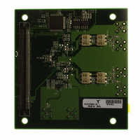
Manufacturer Part Number
KDC5612EVAL
Description
DAUGHTER CARD FOR KAD5612
Manufacturer
Intersil
Series
FemtoCharge™r
Datasheets
1.KAD5612P-25Q72.pdf
(29 pages)
2.KMB-001LEVALZ.pdf
(7 pages)
3.KDC5514EVALZ.pdf
(9 pages)
Specifications of KDC5612EVAL
Number Of Adc's
2
Number Of Bits
12
Sampling Rate (per Second)
250M
Data Interface
Parallel
Inputs Per Adc
1 Differential
Input Range
1.47 Vpp
Power (typ) @ Conditions
429mW @ 250MSPS
Voltage Supply Source
Single Supply
Operating Temperature
-40°C ~ 85°C
Utilized Ic / Part
KAD5612P-25, KMB001 Motherboard
For Use With
KMB001LEVAL - MOTHERBOARD FOR LVDS ADC CARD
Lead Free Status / RoHS Status
Lead free / RoHS Compliant


A delay-locked loop (DLL) generates internal clock signals
for various stages within the charge pipeline. If the frequency
of the input clock changes, the DLL may take up to 52µs to
regain lock at 250MSPS. The lock time is inversely
proportional to the sample rate.
Jitter
In a sampled data system, clock jitter directly impacts the
achievable SNR performance. The theoretical relationship
between clock jitter (t
is illustrated in Figure 31.
This relationship shows the SNR that would be achieved if
clock jitter were the only non-ideal factor. In reality,
achievable SNR is limited by internal factors such as
linearity, aperture jitter and thermal noise. Internal aperture
jitter is the uncertainty in the sampling instant shown in
Figure 1. The internal aperture jitter combines with the input
clock jitter in a root-sum-square fashion, since they are not
statistically correlated, and this determines the total jitter in
the system. The total jitter, combined with other noise
sources, then determines the achievable SNR.
Voltage Reference
A temperature compensated voltage reference provides the
reference charges used in the successive approximation
operations. The full-scale range of each A/D is proportional
to the reference voltage. The nominal value of the voltage
reference is 1.25V.
Digital Outputs
Output data is available as a parallel bus in
LVDS-compatible or CMOS modes. In either case, the data
is presented in double data rate (DDR) format with the A and
B channel data available on alternating clock edges. When
CLKOUT is low channel A data is output, while on the high
phase channel B data is presented. Figures 1 and 2 show
the timing relationships for LVDS and CMOS modes,
respectively.
SNR
100
95
90
85
80
75
70
65
60
55
50
1M
=
20 log
FIGURE 31. SNR vs CLOCK JITTER
10
tj = 100ps
⎛
⎝
------------------- -
2πf
1
IN
J
t
) and SNR is shown in Equation 1 and
INPUT FREQUENCY (Hz)
J
10M
⎞
⎠
tj = 10ps
17
tj = 1ps
tj = 0.1ps
100M
10 BITS
14 BITS
12 BITS
(EQ. 1)
KAD5612P
1G
Additionally, the drive current for LVDS mode can be set to a
nominal 3mA or a power-saving 2mA. The lower current
setting can be used in designs where the receiver is in close
physical proximity to the ADC. The applicability of this setting
is dependent upon the PCB layout, therefore the user should
experiment to determine if performance degradation is
observed.
The output mode and LVDS drive current are selected via
the OUTMODE pin as shown in Table 2.
The output mode can also be controlled through the SPI
port, which overrides the OUTMODE pin setting. Details on
this are contained in “Serial Peripheral Interface” on
page 19.
An external resistor creates the bias for the LVDS drivers. A
10kΩ, 1% resistor must be connected from the RLVDS pin to
OVSS.
Over Range Indicator
The over range (OR) bit is asserted when the output code
reaches positive full-scale (e.g. 0xFFF in offset binary
mode). The output code does not wrap around during an
over range condition. The OR bit is updated at the sample
rate.
Power Dissipation
The power dissipated by the KAD5612P is primarily
dependent on the sample rate and the output modes: LVDS
vs. CMOS and DDR vs. SDR. There is a static bias in the
analog supply, while the remaining power dissipation is
linearly related to the sample rate. The output supply
dissipation changes to a lesser degree in LVDS mode, but is
more strongly related to the clock frequency in CMOS mode.
Nap/Sleep
Portions of the device may be shut down to save power during
times when operation of the ADC is not required. Two power
saving modes are available: Nap, and Sleep. Nap mode
reduces power dissipation to less than 163mW and recovers
to normal operation in approximately 1µs. Sleep mode
reduces power dissipation to less than 6mW but requires
approximately 1ms to recover from a sleep command.
Wake-up time from sleep mode is dependent on the state of
CSB; in a typical application CSB would be held high during
sleep, requiring a user to wait 150µs max after CSB is
asserted (brought low) prior to writing ‘001x’ to SPI register
25. The device would be fully powered up, in normal mode
1ms after this command is written.
OUTMODE PIN
AVDD
AVSS
Float
TABLE 2. OUTMODE PIN SETTINGS
LVDS, 3mA
LVDS, 2mA
LVCMOS
MODE
September 9, 2009
FN6803.2
Related parts for KDC5612EVAL
Image
Part Number
Description
Manufacturer
Datasheet
Request
R

Part Number:
Description:
Intersil Corporation [CMOS Serial Controller Interface]
Manufacturer:
Intersil Corporation
Datasheet:
Part Number:
Description:
Manufacturer:
Intersil Corporation
Datasheet:
Part Number:
Description:
357-036-542-201 CARDEDGE 36POS DL .156 BLK LOPRO
Manufacturer:
Intersil Corporation
Datasheet:
Part Number:
Description:
1024-Word x 4-Bit LSI Static RAM
Manufacturer:
Intersil Corporation
Datasheet:
Part Number:
Description:
General Purpose NPN Transistor Arrays FN341.4
Manufacturer:
Intersil Corporation
Datasheet:
Part Number:
Description:
CMOS 16-Bit Microprocessor
Manufacturer:
Intersil Corporation
Datasheet:
Part Number:
Description:
Manufacturer:
Intersil Corporation
Datasheet:
Part Number:
Description:
Manufacturer:
Intersil Corporation
Datasheet:
Part Number:
Description:
Manufacturer:
Intersil Corporation
Datasheet:
Part Number:
Description:
Manufacturer:
Intersil Corporation
Datasheet:
Part Number:
Description:
CMOS 6-Bit Latch and Decoder Memory Interfaces
Manufacturer:
Intersil Corporation
Datasheet:
Part Number:
Description:
CA3046General Purpose NPN Transistor Arrays
Manufacturer:
Intersil Corporation
Datasheet:
Part Number:
Description:
Manufacturer:
Intersil Corporation
Datasheet:
Part Number:
Description:
TR909 DLC/FLC SLIC with Low Power Standby
Manufacturer:
Intersil Corporation
Datasheet:
Part Number:
Description:
Manufacturer:
Intersil Corporation
Datasheet: