KDC5612EVAL Intersil, KDC5612EVAL Datasheet - Page 28
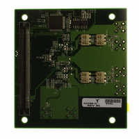
KDC5612EVAL
Manufacturer Part Number
KDC5612EVAL
Description
DAUGHTER CARD FOR KAD5612
Manufacturer
Intersil
Series
FemtoCharge™r
Datasheets
1.KAD5612P-25Q72.pdf
(29 pages)
2.KMB-001LEVALZ.pdf
(7 pages)
3.KDC5514EVALZ.pdf
(9 pages)
Specifications of KDC5612EVAL
Number Of Adc's
2
Number Of Bits
12
Sampling Rate (per Second)
250M
Data Interface
Parallel
Inputs Per Adc
1 Differential
Input Range
1.47 Vpp
Power (typ) @ Conditions
429mW @ 250MSPS
Voltage Supply Source
Single Supply
Operating Temperature
-40°C ~ 85°C
Utilized Ic / Part
KAD5612P-25, KMB001 Motherboard
For Use With
KMB001LEVAL - MOTHERBOARD FOR LVDS ADC CARD
Lead Free Status / RoHS Status
Lead free / RoHS Compliant


Revision History
Intersil products are sold by description only. Intersil Corporation reserves the right to make changes in circuit design, software and/or specifications at any time without
notice. Accordingly, the reader is cautioned to verify that data sheets are current before placing orders. Information furnished by Intersil is believed to be accurate and
reliable. However, no responsibility is assumed by Intersil or its subsidiaries for its use; nor for any infringements of patents or other rights of third parties which may result
from its use. No license is granted by implication or otherwise under any patent or patent rights of Intersil or its subsidiaries.
7/30/08
12/5/08
1/21/09
5/07/09
8/21/09
DATE
8/4/09
REVISION
FN6803.0 Converted to intersil template. Assigned file number FN6803. Rev 0 - first release with new file number.
FN6803.1 P1; revised Key Specs
FN6803.2 1) Updated pin diagram; Added nap mode, sleep mode wake up times to spec table
All Intersil U.S. products are manufactured, assembled and tested utilizing ISO9000 quality systems.
Rev 1
Intersil Corporation’s quality certifications can be viewed at www.intersil.com/design/quality
For information regarding Intersil Corporation and its products, see www.intersil.com
Initial Release of Production Datasheet
P2; added Part Marking column to Order Info
P4; Moved Thermal Impedance under Thermal Info (used to be on p. 7). Added Theta JA Note 2.
P4-7; edits throughout the Specs table. Added Notes 8 and 9. Revised Notes 6 and 7.
P7; Removed ESD section
P10-12; revised Performance Curves throughout
P14; User Inititated Reset section; revised 2nd sentence of 1st paragraph
P18; SPI Physical Interface; revised 3nd sentence of 1st paragraph. “SPI Physical Interface”; revised 2nd sentence of
4th paragraph.
P20; added last 2 sentences to 1st paragraph of "ADDRESS 0X24: GAIN_FINE". Revised Table 8
P21; revised last 2 sentence of "ADDRESS 0X71: PHASE_SLIP". Removed Figure of "PHASE SLIP: CLK÷2 MODE,
fCLOCK = 500MHz"
P24; revised Figure 44
P24; Table 17; revised Bits7:4, Addr C0
Throughout; formatted graphics to Intersil standards
2) Added CSB,SCLK Setup time specs for nap, sleep modes to spec table
4) Changed SPI setup spec wording in spec table
5) Change to pin description table for clarification
6) Added thermal pad note
7) Updated fig 24 and fig 25 and description in text.
8) Update multiple device usage note on at “SPI Physical Interface” on page 19
9) Added ‘Reserved’ to SPI memory map at address 25H
10) Added section on “ADC Evaluation Platform” on page 26
11) Intersil Standards: Added Pb-free reflow link to thermal information, moved caution statement above note to follow
format, added note reference for over-temp note in Elec Spec Tables and added over-temp note at end of table, updated
Table of Contents.
1. Change to SPI interface section in spec table, timing in cycles now, added write, read specific timing specs
2. Updated SPI timing diagrams, Figures 36, 37
3. Updated wakeup time description in “Nap/Sleep” on page 17.
4. Removed calibration note in spec table
1. Fig 43.changed 2 resistors between inputs from 11 ohms to 11k ohms.
2. Fig 45. moved 20k ohm label upwards a bit
3. Page 15, reword the end of the paragraph above Figure 24
4. Changed tDHR spec on p7 from 1.5cycles to 3 cycles.
28
KAD5612P
CHANGE
September 9, 2009
FN6803.2
Related parts for KDC5612EVAL
Image
Part Number
Description
Manufacturer
Datasheet
Request
R

Part Number:
Description:
Intersil Corporation [CMOS Serial Controller Interface]
Manufacturer:
Intersil Corporation
Datasheet:
Part Number:
Description:
Manufacturer:
Intersil Corporation
Datasheet:
Part Number:
Description:
357-036-542-201 CARDEDGE 36POS DL .156 BLK LOPRO
Manufacturer:
Intersil Corporation
Datasheet:
Part Number:
Description:
1024-Word x 4-Bit LSI Static RAM
Manufacturer:
Intersil Corporation
Datasheet:
Part Number:
Description:
General Purpose NPN Transistor Arrays FN341.4
Manufacturer:
Intersil Corporation
Datasheet:
Part Number:
Description:
CMOS 16-Bit Microprocessor
Manufacturer:
Intersil Corporation
Datasheet:
Part Number:
Description:
Manufacturer:
Intersil Corporation
Datasheet:
Part Number:
Description:
Manufacturer:
Intersil Corporation
Datasheet:
Part Number:
Description:
Manufacturer:
Intersil Corporation
Datasheet:
Part Number:
Description:
Manufacturer:
Intersil Corporation
Datasheet:
Part Number:
Description:
CMOS 6-Bit Latch and Decoder Memory Interfaces
Manufacturer:
Intersil Corporation
Datasheet:
Part Number:
Description:
CA3046General Purpose NPN Transistor Arrays
Manufacturer:
Intersil Corporation
Datasheet:
Part Number:
Description:
Manufacturer:
Intersil Corporation
Datasheet:
Part Number:
Description:
TR909 DLC/FLC SLIC with Low Power Standby
Manufacturer:
Intersil Corporation
Datasheet:
Part Number:
Description:
Manufacturer:
Intersil Corporation
Datasheet: