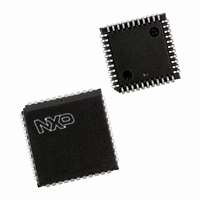
P89V52X2FA,512 NXP Semiconductors, P89V52X2FA,512 Datasheet - Page 30

P89V52X2FA,512
Manufacturer Part Number
P89V52X2FA,512
Description
IC 80C51 MCU FLASH 8K 44-PLCC
Manufacturer
NXP Semiconductors
Series
89Vr
Datasheet
1.P89V52X2FA512.pdf
(57 pages)
Specifications of P89V52X2FA,512
Program Memory Type
FLASH
Program Memory Size
8KB (8K x 8)
Package / Case
44-PLCC
Core Processor
8051
Core Size
8-Bit
Speed
40MHz
Connectivity
UART/USART
Peripherals
POR
Number Of I /o
32
Eeprom Size
192 x 8
Ram Size
256 x 8
Voltage - Supply (vcc/vdd)
2.7 V ~ 5.5 V
Oscillator Type
External
Operating Temperature
-40°C ~ 85°C
Processor Series
P89V5x
Core
80C51
Data Bus Width
8 bit
Data Ram Size
256 B
Interface Type
UART
Maximum Clock Frequency
40 MHz
Number Of Programmable I/os
32
Number Of Timers
3
Operating Supply Voltage
2.7 V to 5.5 V
Maximum Operating Temperature
+ 125 C
Mounting Style
SMD/SMT
3rd Party Development Tools
PK51, CA51, A51, ULINK2
Minimum Operating Temperature
- 55 C
Lead Free Status / RoHS Status
Lead free / RoHS Compliant
For Use With
OM11011 - BOARD FOR P89V52X2 44-TQFP622-1017 - BOARD 44-ZIF PLCC SOCKET622-1012 - BOARD FOR P89V52X2 44-TQFP622-1008 - BOARD FOR LPC9103 10-HVSON622-1002 - USB IN-CIRCUIT PROG LPC9XX
Data Converters
-
Lead Free Status / Rohs Status
Lead free / RoHS Compliant
Other names
568-4249-5
935282528512
P89V52X2FA
935282528512
P89V52X2FA
Available stocks
Company
Part Number
Manufacturer
Quantity
Price
Company:
Part Number:
P89V52X2FA,512
Manufacturer:
NXP Semiconductors
Quantity:
10 000
NXP Semiconductors
Table 24.
P89V52X2_3
Product data sheet
Description
External
Interrupt 0
T0
External
Interrupt 1
T1
UART
T2
Interrupt polling sequence
6.11 Interrupt priority and polling sequence
Interrupt flag
IE0
TF0
IE1
TF1
TI/RI
TF2, EXF2
SADDR = 1100 0000
--------------------------------------------------- -
Example 2, slave 1:
SADDR = 1110 0000
--------------------------------------------------- -
Example 2, slave 2:
SADDR = 1100 0000
--------------------------------------------------- -
In the above example the differentiation among the 3 slaves is in the lower 3 address bits.
Slave 0 requires that bit 0 = 0 and it can be uniquely addressed by 1110 0110. Slave 1
requires that bit 1 = 0 and it can be uniquely addressed by 1110 0101. Slave 2 requires
that bit 2 = 0 and its unique address is 1110 0011. To select Slaves 0 and 1 and exclude
Slave 2 use address 1110 0100, since it is necessary to make bit 2 = 1 to exclude slave 2.
The Broadcast Address for each slave is created by taking the logical OR of SADDR and
SADEN. Zeros in this result are treated as don’t-cares. In most cases, interpreting the
don’t-cares as ones, the broadcast address will be FF hexadecimal. Upon reset SADDR
and SADEN are loaded with 0s. This produces a given address of all ‘don’t cares’ as well
as a Broadcast address of all ‘don’t cares'. This effectively disables the Automatic
Addressing mode and allows the microcontroller to use standard UART drivers which do
not make use of this feature.
The device supports six interrupt sources under a four level priority scheme.
summarizes the polling sequence of the supported interrupts. (See
SADEN = 1111 1001
SADEN = 1111 1010
SADEN = 1111 1100
Given = 1100 0XX0
Given = 1110 0X0X
Given = 1100 00XX
Vector address Interrupt
0003H
000BH
0013H
001BH
0023H
003BH
Rev. 03 — 4 May 2009
enable
EX0
ET0
EX1
ET1
ES0
ET2
Interrupt
priority
PX0/H
PT0/H
PX1/H
PT1/H
PS0/H
PT2/H
80C51 with 256 B RAM, 192 B data EEPROM
Service
priority
1 (highest)
2
3
4
5
6
Figure
P89V52X2
© NXP B.V. 2009. All rights reserved.
Wake-up
Power-down
yes
no
yes
no
no
no
19).
Table 24
30 of 57
(6)
(7)
(8)


