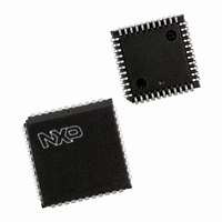
P89V52X2FA,512 NXP Semiconductors, P89V52X2FA,512 Datasheet - Page 36

P89V52X2FA,512
Manufacturer Part Number
P89V52X2FA,512
Description
IC 80C51 MCU FLASH 8K 44-PLCC
Manufacturer
NXP Semiconductors
Series
89Vr
Datasheet
1.P89V52X2FA512.pdf
(57 pages)
Specifications of P89V52X2FA,512
Program Memory Type
FLASH
Program Memory Size
8KB (8K x 8)
Package / Case
44-PLCC
Core Processor
8051
Core Size
8-Bit
Speed
40MHz
Connectivity
UART/USART
Peripherals
POR
Number Of I /o
32
Eeprom Size
192 x 8
Ram Size
256 x 8
Voltage - Supply (vcc/vdd)
2.7 V ~ 5.5 V
Oscillator Type
External
Operating Temperature
-40°C ~ 85°C
Processor Series
P89V5x
Core
80C51
Data Bus Width
8 bit
Data Ram Size
256 B
Interface Type
UART
Maximum Clock Frequency
40 MHz
Number Of Programmable I/os
32
Number Of Timers
3
Operating Supply Voltage
2.7 V to 5.5 V
Maximum Operating Temperature
+ 125 C
Mounting Style
SMD/SMT
3rd Party Development Tools
PK51, CA51, A51, ULINK2
Minimum Operating Temperature
- 55 C
Lead Free Status / RoHS Status
Lead free / RoHS Compliant
For Use With
OM11011 - BOARD FOR P89V52X2 44-TQFP622-1017 - BOARD 44-ZIF PLCC SOCKET622-1012 - BOARD FOR P89V52X2 44-TQFP622-1008 - BOARD FOR LPC9103 10-HVSON622-1002 - USB IN-CIRCUIT PROG LPC9XX
Data Converters
-
Lead Free Status / Rohs Status
Lead free / RoHS Compliant
Other names
568-4249-5
935282528512
P89V52X2FA
935282528512
P89V52X2FA
Available stocks
Company
Part Number
Manufacturer
Quantity
Price
Company:
Part Number:
P89V52X2FA,512
Manufacturer:
NXP Semiconductors
Quantity:
10 000
NXP Semiconductors
Table 33.
P89V52X2_3
Product data sheet
Bit
Symbol (R)
Symbol (W)
Reset
Flash Memory Control register (FMCON - address F4H) bit allocation
FMCMD.7
BUSY
7
0
Writing either the PROG or EP command to FMCON will start the program or
erase-program process and place the CPU in a program-idle state. The CPU will remain
in this idle state until the program or erase-program cycle is completed. Interrupts will NOT
be serviced until the cycle is completed.
Erase-program or programming of a single byte (or multiple bytes) in the data EEPROM
array is accomplished using the following steps:
•
•
•
•
•
•
•
•
•
Write the LOAD command (00H) to FMCON. The LOAD command will clear all
locations in the page register and their corresponding update flags.
Write the address within the page register to FMADRL. Since the loading the page
register uses FMADRL[5:0], and since the erase-program or program command uses
FMADRH and FMADRL[7:6], the user can write the byte location within the page
register (FMADRL[5:0]) and the code memory page address (FMADRH and
FMADRL[7:6]) at this time.
Write the data to be programmed to FMDATA. This will increment FMADRL pointing to
the next byte in the page register.
Write the address of the next byte to be programmed to FMADRL, if desired. (This is
not needed for contiguous bytes since FMADRL is auto-incremented). All bytes to be
programmed must be within the same page.
Write the data for the next byte to be programmed to FMDATA.
Repeat writing of FMADRL and/or FMDATA until all desired bytes have been loaded
into the page register.
Write the page address mapped into user code memory to FMADRH and
FMADRL[7:6], if not previously included when writing the page register address to
FMADRL[5:0].
Write the EP (68H) or PROG (48H) command to FMCON, starting the erase-program
or program cycle.
Read FMCON to check status. If aborted, repeat starting with the LOAD command.
FMCMD.6
WE
6
0
FMCMD.5
5
0
-
Rev. 03 — 4 May 2009
FMCMD.4
DAP
4
0
FMCMD.3
80C51 with 256 B RAM, 192 B data EEPROM
3
0
-
FMCMD.2
2
0
-
FMCMD.1
P89V52X2
SV
1
0
© NXP B.V. 2009. All rights reserved.
FMCMD.0
ERR
0
0
36 of 57


