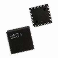
P89V52X2FA,512 NXP Semiconductors, P89V52X2FA,512 Datasheet - Page 6

P89V52X2FA,512
Manufacturer Part Number
P89V52X2FA,512
Description
IC 80C51 MCU FLASH 8K 44-PLCC
Manufacturer
NXP Semiconductors
Series
89Vr
Datasheet
1.P89V52X2FA512.pdf
(57 pages)
Specifications of P89V52X2FA,512
Program Memory Type
FLASH
Program Memory Size
8KB (8K x 8)
Package / Case
44-PLCC
Core Processor
8051
Core Size
8-Bit
Speed
40MHz
Connectivity
UART/USART
Peripherals
POR
Number Of I /o
32
Eeprom Size
192 x 8
Ram Size
256 x 8
Voltage - Supply (vcc/vdd)
2.7 V ~ 5.5 V
Oscillator Type
External
Operating Temperature
-40°C ~ 85°C
Processor Series
P89V5x
Core
80C51
Data Bus Width
8 bit
Data Ram Size
256 B
Interface Type
UART
Maximum Clock Frequency
40 MHz
Number Of Programmable I/os
32
Number Of Timers
3
Operating Supply Voltage
2.7 V to 5.5 V
Maximum Operating Temperature
+ 125 C
Mounting Style
SMD/SMT
3rd Party Development Tools
PK51, CA51, A51, ULINK2
Minimum Operating Temperature
- 55 C
Lead Free Status / RoHS Status
Lead free / RoHS Compliant
For Use With
OM11011 - BOARD FOR P89V52X2 44-TQFP622-1017 - BOARD 44-ZIF PLCC SOCKET622-1012 - BOARD FOR P89V52X2 44-TQFP622-1008 - BOARD FOR LPC9103 10-HVSON622-1002 - USB IN-CIRCUIT PROG LPC9XX
Data Converters
-
Lead Free Status / Rohs Status
Lead free / RoHS Compliant
Other names
568-4249-5
935282528512
P89V52X2FA
935282528512
P89V52X2FA
Available stocks
Company
Part Number
Manufacturer
Quantity
Price
Company:
Part Number:
P89V52X2FA,512
Manufacturer:
NXP Semiconductors
Quantity:
10 000
NXP Semiconductors
Table 2.
P89V52X2_3
Product data sheet
Symbol
P1[7]
P2[0] to P2[7]
P2[0]/A8
P2[1]/A9
P2[2]/A10
P2[3]/A11
P2[4]/A12
P2[5]/A13
P2[6]/A14
P2[7]/A15
P3[0] to P3[7]
P3[0]/RXD
P3[1]/TXD
P3[2]/INT0
P3[3]/INT1
P3[4]/T0
Pin description
Pin
DIP40
8
21
22
23
24
25
26
27
28
10
11
12
13
14
…continued
LQFP44
3
18
19
20
21
22
23
24
25
5
7
8
9
10
PLCC44
9
24
25
26
27
28
29
30
31
11
13
14
15
16
Rev. 03 — 4 May 2009
Type
I/O
I/O with
internal
pull-up
I/O
O
I/O
O
I/O
O
I/O
O
I/O
O
I/O
O
I/O
O
I/O
O
I/O
with
internal
pull-up
I
I
O
O
I
I
I
I
I/O
I
Description
P1[7] — Port 1 bit 7.
Port 2: Port 2 is an 8-bit bidirectional I/O port with internal
pull-ups. Port 2 pins are pulled HIGH by the internal
pull-ups when ‘1’s are written to them and can be used as
inputs in this state. As inputs, Port 2 pins that are
externally pulled LOW will source current (I
the internal pull-ups. Port 2 sends the high-order address
byte during fetches from external program memory and
during accesses to external Data Memory that use 16-bit
address (MOVX@DPTR). In this application, it uses strong
internal pull-ups when transitioning to ‘1’s.
P2[0] — Port 2 bit 0.
A8 — Address bit 8.
P2[1] — Port 2 bit 1.
A9 — Address bit 9.
P2[2] — Port 2 bit 2.
A10 — Address bit 10.
P2[3] — Port 2 bit 3.
A11 — Address bit 11.
P2[4] — Port 2 bit 4.
A12 — Address bit 12.
P2[5] — Port 2 bit 5.
A13 — Address bit 13.
P2[6] — Port 2 bit 6.
A14 — Address bit 14.
P2[7] — Port 2 bit 7.
A15 — Address bit 15.
Port 3: Port 3 is an 8-bit bidirectional I/O port with internal
pull-ups. Port 3 pins are pulled HIGH by the internal
pull-ups when ‘1’s are written to them and can be used as
inputs in this state. As inputs, Port 3 pins that are
externally pulled LOW will source current (I
the internal pull-ups.
P3[0] — Port 3 bit 0.
RXD — Serial input port.
P3[1] — Port 3 bit 1.
TXD — Serial output port.
P3[2] — Port 3 bit 2.
INT0 — External interrupt 0 input.
P3[3] — Port 3 bit 3.
INT1 — External interrupt 1 input
P3[4] — Port 3 bit 4.
T0 — External count input to Timer/Counter 0.
80C51 with 256 B RAM, 192 B data EEPROM
P89V52X2
© NXP B.V. 2009. All rights reserved.
IL
IL
) because of
) because of
6 of 57


