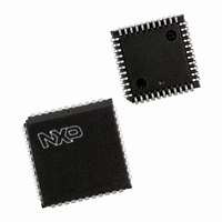
P89V52X2FA,512 NXP Semiconductors, P89V52X2FA,512 Datasheet - Page 34

P89V52X2FA,512
Manufacturer Part Number
P89V52X2FA,512
Description
IC 80C51 MCU FLASH 8K 44-PLCC
Manufacturer
NXP Semiconductors
Series
89Vr
Datasheet
1.P89V52X2FA512.pdf
(57 pages)
Specifications of P89V52X2FA,512
Program Memory Type
FLASH
Program Memory Size
8KB (8K x 8)
Package / Case
44-PLCC
Core Processor
8051
Core Size
8-Bit
Speed
40MHz
Connectivity
UART/USART
Peripherals
POR
Number Of I /o
32
Eeprom Size
192 x 8
Ram Size
256 x 8
Voltage - Supply (vcc/vdd)
2.7 V ~ 5.5 V
Oscillator Type
External
Operating Temperature
-40°C ~ 85°C
Processor Series
P89V5x
Core
80C51
Data Bus Width
8 bit
Data Ram Size
256 B
Interface Type
UART
Maximum Clock Frequency
40 MHz
Number Of Programmable I/os
32
Number Of Timers
3
Operating Supply Voltage
2.7 V to 5.5 V
Maximum Operating Temperature
+ 125 C
Mounting Style
SMD/SMT
3rd Party Development Tools
PK51, CA51, A51, ULINK2
Minimum Operating Temperature
- 55 C
Lead Free Status / RoHS Status
Lead free / RoHS Compliant
For Use With
OM11011 - BOARD FOR P89V52X2 44-TQFP622-1017 - BOARD 44-ZIF PLCC SOCKET622-1012 - BOARD FOR P89V52X2 44-TQFP622-1008 - BOARD FOR LPC9103 10-HVSON622-1002 - USB IN-CIRCUIT PROG LPC9XX
Data Converters
-
Lead Free Status / Rohs Status
Lead free / RoHS Compliant
Other names
568-4249-5
935282528512
P89V52X2FA
935282528512
P89V52X2FA
Available stocks
Company
Part Number
Manufacturer
Quantity
Price
Company:
Part Number:
P89V52X2FA,512
Manufacturer:
NXP Semiconductors
Quantity:
10 000
NXP Semiconductors
P89V52X2_3
Product data sheet
6.13.1 Features
6.13.2 Register interface
6.13.3 Mapping the data EEPROM into code space
6.13.4 Reading the data EEPROM
The data EEPROM must be mapped into the code memory address space in order to
read, erase, or program the data EEPROM. The memory is read using the MOVC
instruction.
Erasing, programming, and mapping operations are performed in the application under
the control of the microcontroller’s firmware using four SFRs and an internal 64-byte ‘page
register’. These SFRs are:
Data is read by mapping the data EEPROM into the code memory space and using the
MOVC instruction.
In order to read, erase, or program the data EEPROM must be mapped into the code
memory address space. This is accomplished by writing the MAP command (09H) to
FMCON. The data EEPROM may be unmapped by writing the UNMAP command (0AH)
to FMCON. The mapping of the data EEPROM pages into code memory space is shown
in
Table 32.
Reading the data EEPROM can be achieved by performing the following sequence:
Data EEPROM page
0
1
2
•
•
•
•
•
•
•
•
•
•
•
Table
ICP with industry-standard commercial programmers
IAP-Lite allows individual and multiple bytes of data EEPROM to be programmed
under control of the end application.
Programming and erase over the full operating voltage range
Programming/Erase using ICP or IAP-Lite
Program or erases requires 2 ms, 4 ms, or 6 ms, depending on the operation
Programmable security for the data in each page
> 100000 typical erase/program cycles for each byte
Data EEPROM mapped into code space for quick MOVC reading
FMCON (Flash Control Register). When read, this is the status register. When written,
this is a command register. Note that the status bits are cleared to logic 0s when the
command is written.
FMADRL, FMADRH (Flash memory address low, Flash memory address high). Used
to specify the byte address within the page register or specify the page within user
code memory (for programming, erase, and reading the data EEPROM is mapped
into the user address space (see
FMDATA (Flash Data Register). Accepts data to be loaded into the page register.
32.
Data EEPROM page addresses
Start address End address
FF00H
FF40H
FF80H
Rev. 03 — 4 May 2009
FF3FH
FF7FH
FFBFH
Table
80C51 with 256 B RAM, 192 B data EEPROM
32).
P89V52X2
© NXP B.V. 2009. All rights reserved.
34 of 57


