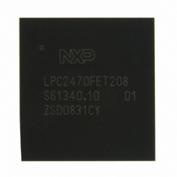
LPC2470FET208,551 NXP Semiconductors, LPC2470FET208,551 Datasheet - Page 80

LPC2470FET208,551
Manufacturer Part Number
LPC2470FET208,551
Description
IC ARM7 MCU LCD 208-TFBGA
Manufacturer
NXP Semiconductors
Series
LPC2400r
Datasheets
1.OM11077.pdf
(792 pages)
2.LPC2470FET208551.pdf
(89 pages)
3.LPC2470FET208551.pdf
(91 pages)
Specifications of LPC2470FET208,551
Package / Case
208-TFBGA
Core Processor
ARM7
Core Size
16/32-Bit
Speed
72MHz
Connectivity
CAN, EBI/EMI, Ethernet, I²C, Microwire, MMC, SPI, SSI, SSP, UART/USART, USB OTG
Peripherals
Brown-out Detect/Reset, DMA, I²S, LCD, POR, PWM, WDT
Number Of I /o
160
Program Memory Type
ROMless
Ram Size
98K x 8
Voltage - Supply (vcc/vdd)
3 V ~ 3.6 V
Data Converters
A/D 8x10b; D/A 1x10b
Oscillator Type
Internal
Operating Temperature
-40°C ~ 85°C
Processor Series
LPC24
Core
ARM7TDMI-S
Data Bus Width
16 bit, 32 bit
Data Ram Size
98 KB
Interface Type
CAN/I2C/I2S/SPI/SSP/UART/USB
Maximum Clock Frequency
72 MHz
Number Of Programmable I/os
160
Number Of Timers
4
Maximum Operating Temperature
+ 85 C
Mounting Style
SMD/SMT
3rd Party Development Tools
MDK-ARM, RL-ARM, ULINK2, MCB2470U
Minimum Operating Temperature
- 40 C
On-chip Adc
8-ch x 10-bit
On-chip Dac
1-ch x 10-bit
Package
208TFBGA
Device Core
ARM7TDMI-S
Family Name
LPC2000
Maximum Speed
72 MHz
Operating Supply Voltage
3.3 V
Lead Free Status / RoHS Status
Lead free / RoHS Compliant
Eeprom Size
-
Program Memory Size
-
Lead Free Status / Rohs Status
Lead free / RoHS Compliant
Other names
568-4362
935284071551
LPC2470FET208-S
935284071551
LPC2470FET208-S
Available stocks
Company
Part Number
Manufacturer
Quantity
Price
Company:
Part Number:
LPC2470FET208,551
Manufacturer:
Exar
Quantity:
92
Company:
Part Number:
LPC2470FET208,551
Manufacturer:
NXP Semiconductors
Quantity:
10 000
NXP Semiconductors
LPC2470
Product data sheet
14.6 XTAL and RTCX Printed Circuit Board (PCB) layout guidelines
14.7 Standard I/O pin configuration
The crystal should be connected on the PCB as close as possible to the oscillator input
and output pins of the chip. Take care that the load capacitors C
third overtone crystal usage have a common ground plane. The external components
must also be connected to the ground plain. Loops must be made as small as possible in
order to keep the noise coupled in via the PCB as small as possible. Also parasitics
should stay as small as possible. Values of C
accordingly to the increase in parasitics of the PCB layout.
Figure 32
The default configuration for standard I/O pins is input with pull-up enabled. The weak
MOS devices provide a drive capability equivalent to pull-up and pull-down resistors.
Fig 32. Standard I/O pin configuration with analog input
•
•
•
•
•
as digital output
as analog input
as digital input
pin configured
pin configured
pin configured
Digital output driver: Open-drain mode enabled/disabled
Digital input: Pull-up enabled/disabled
Digital input: Pull-down enabled/disabled
Digital input: Repeater mode enabled/disabled
Analog input
driver
shows the possible pin modes for standard I/O pins with analog input function:
All information provided in this document is subject to legal disclaimers.
analog input
Rev. 3 — 14 February 2011
data input
output
output enable
pull-down enable
pull-up enable
select analog input
x1
and C
Flashless 16-bit/32-bit microcontroller
x2
should be chosen smaller
V
DD
weak
pull-up
weak
pull-down
x1
, C
x2
, and C
LPC2470
© NXP B.V. 2011. All rights reserved.
V
ESD
DD
ESD
V
SS
x3
in case of
002aaf496
80 of 89
PIN


