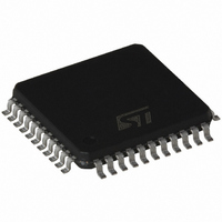
ST72F324BJ6T6 STMicroelectronics, ST72F324BJ6T6 Datasheet - Page 119

ST72F324BJ6T6
Manufacturer Part Number
ST72F324BJ6T6
Description
IC MCU 8BIT 32K FLASH 44-LQFP
Manufacturer
STMicroelectronics
Series
ST7r
Datasheet
1.ST72F324BJ2T6.pdf
(198 pages)
Specifications of ST72F324BJ6T6
Core Processor
ST7
Core Size
8-Bit
Speed
8MHz
Connectivity
SCI, SPI
Peripherals
LVD, POR, PWM, WDT
Number Of I /o
32
Program Memory Size
32KB (32K x 8)
Program Memory Type
FLASH
Ram Size
1K x 8
Voltage - Supply (vcc/vdd)
3.8 V ~ 5.5 V
Data Converters
A/D 12x10b
Oscillator Type
Internal
Operating Temperature
-40°C ~ 85°C
Package / Case
44-TQFP, 44-VQFP
Processor Series
ST72F3x
Core
ST7
Data Bus Width
8 bit
Data Ram Size
1 KB
Interface Type
SCI, SPI
Maximum Clock Frequency
8 MHz
Number Of Programmable I/os
32
Number Of Timers
3
Maximum Operating Temperature
+ 85 C
Mounting Style
SMD/SMT
Development Tools By Supplier
ST7232X-EVAL, ST7MDT20-DVP3, ST7MDT20J-EMU3, STX-RLINK
Minimum Operating Temperature
- 40 C
On-chip Adc
10 bit, 12 Channel
For Use With
497-6421 - BOARD EVAL DGTL BATT CHGR DESIGN497-5046 - KIT TOOL FOR ST7/UPSD/STR7 MCU
Lead Free Status / RoHS Status
Lead free / RoHS Compliant
Eeprom Size
-
Lead Free Status / Rohs Status
Details
Other names
497-5590
Available stocks
Company
Part Number
Manufacturer
Quantity
Price
Company:
Part Number:
ST72F324BJ6T6
Manufacturer:
ON
Quantity:
301
Company:
Part Number:
ST72F324BJ6T6
Manufacturer:
STMicroelectronics
Quantity:
10 000
Company:
Part Number:
ST72F324BJ6T6TR
Manufacturer:
STMicroelectronics
Quantity:
10 000
ST72324B-Auto
Caution:
Receiver muting and wake-up feature
In multiprocessor configurations it is often desirable that only the intended message
recipient should actively receive the full message contents, thus reducing redundant SCI
service overhead for all non-addressed receivers.
The non-addressed devices may be placed in sleep mode by means of the muting function.
Setting the RWU bit by software puts the SCI in sleep mode:
A muted receiver may be awakened by one of the following two ways:
●
●
A receiver wakes up by Idle Line detection when the Receive line has recognized an Idle
Frame. Then the RWU bit is reset by hardware but the Idle bit is not set.
A receiver wakes up by Address Mark detection when it received a ‘1’ as the most significant
bit of a word, thus indicating that the message is an address. The reception of this particular
word wakes up the receiver, resets the RWU bit and sets the RDRF bit, which allows the
receiver to receive this word normally and to use it as an address word.
In Mute mode, do not write to the SCICR2 register. If the SCI is in Mute mode during the
read operation (RWU = 1) and an address mark wake-up event occurs (RWU is reset)
before the write operation, the RWU bit will be set again by this write operation.
Consequently the address byte is lost and the SCI is not woken up from Mute mode.
Parity control
Parity control (generation of parity bit in transmission and parity checking in reception) can
be enabled by setting the PCE bit in the SCICR1 register. Depending on the frame length
defined by the M bit, the possible SCI frame formats are as listed in
Table 59.
1. SB = Start bit, STB = Stop bit, and PB = Parity bit.
2. In case of wake-up by an address mark, the MSB bit of the data is taken into account and not the Parity bit.
All the reception status bits cannot be set.
All the receive interrupts are inhibited.
by Idle Line detection if the Wake bit is reset,
by Address Mark detection if the Wake bit is set.
M bit
0
0
1
1
Frame formats
PCE bit
0
1
0
1
(1)(2)
Doc ID13466 Rev 4
| SB | 8 bit data | STB |
| SB | 7-bit data | PB | STB |
| SB | 9-bit data | STB |
| SB | 8-bit data PB | STB |
SCI frame
Table
On-chip peripherals
59.
119/198


