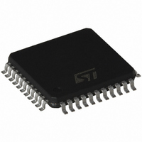
ST72F324BJ6T6 STMicroelectronics, ST72F324BJ6T6 Datasheet - Page 91

ST72F324BJ6T6
Manufacturer Part Number
ST72F324BJ6T6
Description
IC MCU 8BIT 32K FLASH 44-LQFP
Manufacturer
STMicroelectronics
Series
ST7r
Datasheet
1.ST72F324BJ2T6.pdf
(198 pages)
Specifications of ST72F324BJ6T6
Core Processor
ST7
Core Size
8-Bit
Speed
8MHz
Connectivity
SCI, SPI
Peripherals
LVD, POR, PWM, WDT
Number Of I /o
32
Program Memory Size
32KB (32K x 8)
Program Memory Type
FLASH
Ram Size
1K x 8
Voltage - Supply (vcc/vdd)
3.8 V ~ 5.5 V
Data Converters
A/D 12x10b
Oscillator Type
Internal
Operating Temperature
-40°C ~ 85°C
Package / Case
44-TQFP, 44-VQFP
Processor Series
ST72F3x
Core
ST7
Data Bus Width
8 bit
Data Ram Size
1 KB
Interface Type
SCI, SPI
Maximum Clock Frequency
8 MHz
Number Of Programmable I/os
32
Number Of Timers
3
Maximum Operating Temperature
+ 85 C
Mounting Style
SMD/SMT
Development Tools By Supplier
ST7232X-EVAL, ST7MDT20-DVP3, ST7MDT20J-EMU3, STX-RLINK
Minimum Operating Temperature
- 40 C
On-chip Adc
10 bit, 12 Channel
For Use With
497-6421 - BOARD EVAL DGTL BATT CHGR DESIGN497-5046 - KIT TOOL FOR ST7/UPSD/STR7 MCU
Lead Free Status / RoHS Status
Lead free / RoHS Compliant
Eeprom Size
-
Lead Free Status / Rohs Status
Details
Other names
497-5590
Available stocks
Company
Part Number
Manufacturer
Quantity
Price
Company:
Part Number:
ST72F324BJ6T6
Manufacturer:
ON
Quantity:
301
Company:
Part Number:
ST72F324BJ6T6
Manufacturer:
STMicroelectronics
Quantity:
10 000
Company:
Part Number:
ST72F324BJ6T6TR
Manufacturer:
STMicroelectronics
Quantity:
10 000
ST72324B-Auto
Table 50.
Bit
3:2 CC[1:0]
M
7
6
5
4
1
0
EXEDG
IEDG2
Name
OC2E
OCIE
PWM
OPM
CR2 register description
Output Compare 1 Pin Enable
This bit is used only to output the signal from the timer on the OCMP1 pin (OLV1 in
Output Compare mode, both OLV1 and OLV2 in PWM and One-Pulse mode).
Whatever the value of the OC1E bit, the Output Compare 1 function of the timer
remains active.
0: OCMP1 pin alternate function disabled (I/O pin free for general-purpose I/O).
1: OCMP1 pin alternate function enabled.
Output Compare 2 Pin Enable
This bit is used only to output the signal from the timer on the OCMP2 pin (OLV2 in
Output Compare mode). Whatever the value of the OC2E bit, the Output Compare 2
function of the timer remains active.
0: OCMP2 pin alternate function disabled (I/O pin free for general-purpose I/O).
1: OCMP2 pin alternate function enabled.
One Pulse Mode
Pulse Width Modulation
Clock Control
Input Edge 2
External Clock Edge
0: One Pulse mode is not active.
1: One Pulse mode is active, the ICAP1 pin can be used to trigger one pulse on the
OCMP1 pin; the active transition is given by the IEDG1 bit. The length of the
generated pulse depends on the contents of the OC1R register.
0: PWM mode is not active.
1: PWM mode is active, the OCMP1 pin outputs a programmable cyclic signal; the
length of the pulse depends on the value of OC1R register; the period depends on
the value of OC2R register.
The timer clock mode depends on these bits.
00: Timer clock = f
01: Timer clock = f
10: Timer clock = f
11: Timer clock = external clock (where available)
Note: If the external clock pin is not available, programming the external clock
configuration stops the counter.
This bit determines which type of level transition on the ICAP2 pin will trigger the
capture.
0: A falling edge triggers the capture.
1: A rising edge triggers the capture.
This bit determines which type of level transition on the external clock pin EXTCLK
will trigger the counter register.
0: A falling edge triggers the counter register.
1: A rising edge triggers the counter register.
Doc ID13466 Rev 4
CPU
CPU
CPU
/4
/2
/8
Function
On-chip peripherals
91/198


