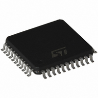
ST72F324BJ6T6 STMicroelectronics, ST72F324BJ6T6 Datasheet - Page 132

ST72F324BJ6T6
Manufacturer Part Number
ST72F324BJ6T6
Description
IC MCU 8BIT 32K FLASH 44-LQFP
Manufacturer
STMicroelectronics
Series
ST7r
Datasheet
1.ST72F324BJ2T6.pdf
(198 pages)
Specifications of ST72F324BJ6T6
Core Processor
ST7
Core Size
8-Bit
Speed
8MHz
Connectivity
SCI, SPI
Peripherals
LVD, POR, PWM, WDT
Number Of I /o
32
Program Memory Size
32KB (32K x 8)
Program Memory Type
FLASH
Ram Size
1K x 8
Voltage - Supply (vcc/vdd)
3.8 V ~ 5.5 V
Data Converters
A/D 12x10b
Oscillator Type
Internal
Operating Temperature
-40°C ~ 85°C
Package / Case
44-TQFP, 44-VQFP
Processor Series
ST72F3x
Core
ST7
Data Bus Width
8 bit
Data Ram Size
1 KB
Interface Type
SCI, SPI
Maximum Clock Frequency
8 MHz
Number Of Programmable I/os
32
Number Of Timers
3
Maximum Operating Temperature
+ 85 C
Mounting Style
SMD/SMT
Development Tools By Supplier
ST7232X-EVAL, ST7MDT20-DVP3, ST7MDT20J-EMU3, STX-RLINK
Minimum Operating Temperature
- 40 C
On-chip Adc
10 bit, 12 Channel
For Use With
497-6421 - BOARD EVAL DGTL BATT CHGR DESIGN497-5046 - KIT TOOL FOR ST7/UPSD/STR7 MCU
Lead Free Status / RoHS Status
Lead free / RoHS Compliant
Eeprom Size
-
Lead Free Status / Rohs Status
Details
Other names
497-5590
Available stocks
Company
Part Number
Manufacturer
Quantity
Price
Company:
Part Number:
ST72F324BJ6T6
Manufacturer:
ON
Quantity:
301
Company:
Part Number:
ST72F324BJ6T6
Manufacturer:
STMicroelectronics
Quantity:
10 000
Company:
Part Number:
ST72F324BJ6T6TR
Manufacturer:
STMicroelectronics
Quantity:
10 000
On-chip peripherals
10.6.3
Note:
132/198
Functional description
The conversion is monotonic, meaning that the result never decreases if the analog input
does not increase.
If the input voltage (V
conversion result is FFh in the ADCDRH register and 03h in the ADCDRL register (without
overflow indication).
If the input voltage (V
conversion result in the ADCDRH and ADCDRL registers is 00 00h.
The A/D converter is linear and the digital result of the conversion is stored in the ADCDRH
and ADCDRL registers. The accuracy of the conversion is described in the Electrical
Characteristics Section.
R
is too high, this will result in a loss of accuracy due to leakage and sampling not being
completed in the allotted time.
A/D converter configuration
The analog input ports must be configured as input, no pull-up, no interrupt. Refer to
Section 9: I/O
to be read as a logic input.
In the ADCCSR register:
Starting the conversion
In the ADCCSR register:
When a conversion is complete:
●
●
A read to the ADCDRH resets the EOC bit.
To read the 10 bits, perform the following steps:
1.
2.
3.
The data is not latched, so both the low and the high data register must be read before the
next conversion is complete. Therefore, it is recommended to disable interrupts while
reading the conversion result.
To read only 8 bits, perform the following steps:
1.
2.
AIN
Select the CS[3:0] bits to assign the analog channel to convert.
Set the ADON bit to enable the A/D converter and to start the conversion. From this
time on, the ADC performs a continuous conversion of the selected channel.
the EOC bit is set by hardware
the result is in the ADCDR registers
Poll the EOC bit.
Read the ADCDRL register
Read the ADCDRH register. This clears EOC automatically.
Poll the EOC bit.
Read the ADCDRH register. This clears EOC automatically.
is the maximum recommended impedance for an analog input signal. If the impedance
ports. Using these pins as analog inputs does not affect the ability of the port
AIN
AIN
) is greater than V
) is lower than V
Doc ID13466 Rev 4
SSA
AREF
(low-level voltage reference) then the
(high-level voltage reference) then the
ST72324B-Auto


