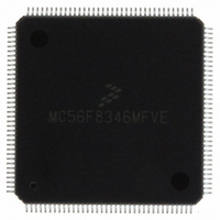
MC56F8346MFVE Freescale Semiconductor, MC56F8346MFVE Datasheet - Page 20

MC56F8346MFVE
Manufacturer Part Number
MC56F8346MFVE
Description
IC DSP 16BIT 60MHZ 144-LQFP
Manufacturer
Freescale Semiconductor
Series
56F8xxxr
Datasheet
1.MC56F8346VFVE.pdf
(178 pages)
Specifications of MC56F8346MFVE
Core Processor
56800
Core Size
16-Bit
Speed
60MHz
Connectivity
CAN, EBI/EMI, SCI, SPI
Peripherals
POR, PWM, Temp Sensor, WDT
Number Of I /o
62
Program Memory Size
136KB (68K x 16)
Program Memory Type
FLASH
Ram Size
6K x 16
Voltage - Supply (vcc/vdd)
2.25 V ~ 3.6 V
Data Converters
A/D 16x12b
Oscillator Type
External
Operating Temperature
-40°C ~ 125°C
Package / Case
144-LQFP
Data Bus Width
16 bit
Processor Series
MC56F83xx
Core
56800E
Numeric And Arithmetic Format
Fixed-Point
Device Million Instructions Per Second
60 MIPs
Maximum Clock Frequency
60 MHz
Number Of Programmable I/os
62
Data Ram Size
4 KB
Operating Supply Voltage
3.6 V
Maximum Operating Temperature
+ 125 C
Mounting Style
SMD/SMT
Interface Type
SCI, SPI, CAN
Minimum Operating Temperature
- 40 C
For Use With
MC56F8367EVME - EVAL BOARD FOR MC56F83X
Lead Free Status / RoHS Status
Lead free / RoHS Compliant
Eeprom Size
-
Lead Free Status / Rohs Status
Lead free / RoHS Compliant
Available stocks
Company
Part Number
Manufacturer
Quantity
Price
Company:
Part Number:
MC56F8346MFVE
Manufacturer:
Freescale
Quantity:
42
Company:
Part Number:
MC56F8346MFVE
Manufacturer:
Freescale Semiconductor
Quantity:
10 000
Part Number:
MC56F8346MFVE
Manufacturer:
FREESCALE
Quantity:
20 000
2.2 Signal Pins
After reset, each pin is configured for its primary function (listed first). Any alternate functionality must
be programmed.
Note: Signals in italics are NOT available in the 56F8146 device.
If the “State During Reset” lists more than one state for a pin, the first state is the actual reset state. Other
states show the reset condition of the alternate function, which you get if the alternate pin function is
selected without changing the configuration of the alternate peripheral. For example, the A8/GPIOA0 pin
shows that it is tri-stated during reset. If the GPIOA_PER is changed to select the GPIO function of the
pin, it will become an input if no other registers are changed.
20
V
Signal Name
DDA_OSC_PLL
V
V
DDA_ADC
SSA_ADC
V
V
V
V
V
V
V
DD_IO
DD_IO
DD_IO
DD_IO
DD_IO
DD_IO
DD_IO
V
V
V
V
V
SS
SS
SS
SS
SS
Table 2-2 Signal and Package Information for the 144 Pin LQFP
Pin No.
119
102
144
103
16
31
38
66
84
80
27
37
63
69
1
Supply
Supply
Supply
Supply
Supply
Type
During
56F8346 Technical Data, Rev. 15
Reset
State
I/O Power — This pin supplies 3.3V power to the chip I/O interface
and also the Processor core throught the on-chip voltage regulator,
if it is enabled.
ADC Power — This pin supplies 3.3V power to the ADC modules.
It must be connected to a clean analog power supply.
Oscillator and PLL Power — This pin supplies 3.3V power to the
OSC and to the internal regulator that in turn supplies the Phase
Locked Loop. It must be connected to a clean analog power
supply.
V
ADC Analog Ground — This pin supplies an analog ground to the
ADC modules.
SS
— These pins provide ground for chip logic and I/O drivers.
Signal Description
Freescale Semiconductor
Preliminary


