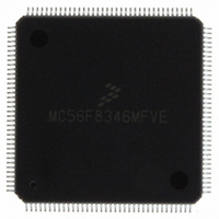
MC56F8346MFVE Freescale Semiconductor, MC56F8346MFVE Datasheet - Page 29

MC56F8346MFVE
Manufacturer Part Number
MC56F8346MFVE
Description
IC DSP 16BIT 60MHZ 144-LQFP
Manufacturer
Freescale Semiconductor
Series
56F8xxxr
Datasheet
1.MC56F8346VFVE.pdf
(178 pages)
Specifications of MC56F8346MFVE
Core Processor
56800
Core Size
16-Bit
Speed
60MHz
Connectivity
CAN, EBI/EMI, SCI, SPI
Peripherals
POR, PWM, Temp Sensor, WDT
Number Of I /o
62
Program Memory Size
136KB (68K x 16)
Program Memory Type
FLASH
Ram Size
6K x 16
Voltage - Supply (vcc/vdd)
2.25 V ~ 3.6 V
Data Converters
A/D 16x12b
Oscillator Type
External
Operating Temperature
-40°C ~ 125°C
Package / Case
144-LQFP
Data Bus Width
16 bit
Processor Series
MC56F83xx
Core
56800E
Numeric And Arithmetic Format
Fixed-Point
Device Million Instructions Per Second
60 MIPs
Maximum Clock Frequency
60 MHz
Number Of Programmable I/os
62
Data Ram Size
4 KB
Operating Supply Voltage
3.6 V
Maximum Operating Temperature
+ 125 C
Mounting Style
SMD/SMT
Interface Type
SCI, SPI, CAN
Minimum Operating Temperature
- 40 C
For Use With
MC56F8367EVME - EVAL BOARD FOR MC56F83X
Lead Free Status / RoHS Status
Lead free / RoHS Compliant
Eeprom Size
-
Lead Free Status / Rohs Status
Lead free / RoHS Compliant
Available stocks
Company
Part Number
Manufacturer
Quantity
Price
Company:
Part Number:
MC56F8346MFVE
Manufacturer:
Freescale
Quantity:
42
Company:
Part Number:
MC56F8346MFVE
Manufacturer:
Freescale Semiconductor
Quantity:
10 000
Part Number:
MC56F8346MFVE
Manufacturer:
FREESCALE
Quantity:
20 000
Freescale Semiconductor
Preliminary
Signal Name
PHASEA0
(GPIOC4)
TRST
(TA0)
TDO
Table 2-2 Signal and Package Information for the 144 Pin LQFP
Pin No.
124
120
139
Schmitt
Schmitt
Schmitt
Schmitt
Output
Output
Output
Input/
Input/
Type
Input
Input
pulled high
disabled,
pull-up is
internally
output is
In reset,
enabled
enabled
During
pull-up
56F8346 Technical Data, Rev. 15
Reset
Input,
Input,
State
Test Data Output — This tri-stateable output pin provides a serial
output data stream from the JTAG/EOnCE port. It is driven in the
shift-IR and shift-DR controller states, and changes on the falling
edge of TCK.
Test Reset — As an input, a low signal on this pin provides a reset
signal to the JTAG TAP controller. To ensure complete hardware
reset, TRST should be asserted whenever RESET is asserted. The
only exception occurs in a debugging environment when a
hardware device reset is required and the JTAG/EOnCE module
must not be reset. In this case, assert RESET, but do not assert
TRST.
To deactivate the internal pull-up resistor, set the JTAG bit in the
SIM_PUDR register.
Note:
design is to be used in a debugging environment, TRST may be tied to
V
Phase A — Quadrature Decoder 0, PHASEA input
TA0 — Timer A, Channel 0
Port C GPIO — This GPIO pin can be individually programmed as
an input or output pin.
After reset, the default state is PHASEA0.
To deactivate the internal pull-up resistor, clear bit 4 of the
GPIOC_PUR register.
SS
through a 1K resistor.
For normal operation, connect TRST directly to V
Signal Description
SS
. If the
Signal Pins
29


