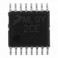
MCL908QY2CDTE Freescale Semiconductor, MCL908QY2CDTE Datasheet - Page 35

MCL908QY2CDTE
Manufacturer Part Number
MCL908QY2CDTE
Description
IC MCU 8BIT 1.5K FLASH 16-TSSOP
Manufacturer
Freescale Semiconductor
Series
HC08r
Datasheet
1.MCL908QY2CDWE.pdf
(182 pages)
Specifications of MCL908QY2CDTE
Core Processor
HC08
Core Size
8-Bit
Speed
2MHz
Peripherals
LVD, POR, PWM
Number Of I /o
13
Program Memory Size
1.5KB (1.5K x 8)
Program Memory Type
FLASH
Ram Size
128 x 8
Voltage - Supply (vcc/vdd)
2.4 V ~ 3.6 V
Data Converters
A/D 4x8b
Oscillator Type
Internal
Operating Temperature
-40°C ~ 85°C
Package / Case
16-TSSOP
Lead Free Status / RoHS Status
Lead free / RoHS Compliant
Eeprom Size
-
Connectivity
-
- Current page: 35 of 182
- Download datasheet (2Mb)
This program sequence is repeated throughout the memory until all data is programmed.
2.6.5 FLASH Protection
Due to the ability of the on-board charge pump to erase and program the FLASH memory in the target
application, provision is made to protect blocks of memory from unintentional erase or program operations
due to system malfunction. This protection is done by use of a FLASH block protect register (FLBPR).
The FLBPR determines the range of the FLASH memory which is to be protected. The range of the
protected area starts from a location defined by FLBPR and ends to the bottom of the FLASH memory
($FFFF). When the memory is protected, the HVEN bit cannot be set in either ERASE or PROGRAM
operations.
When the FLBPR is programmed with all 0s, the entire memory is protected from being programmed and
erased. When all the bits are erased (all 1s), the entire memory is accessible for program and erase.
When bits within the FLBPR are programmed, they lock a block of memory. The address ranges are
shown in
$FF, any erase or program of the FLBPR or the protected block of FLASH memory is prohibited. Mass
erase is disabled whenever any block is protected (FLBPR does not equal $FF). The FLBPR itself can be
erased or programmed only with an external voltage, V
allows entry from reset into the monitor mode.
Freescale Semiconductor
10. Clear the PGM bit
11. Wait for time, t
12. Clear the HVEN bit.
13. After time, t
8. Wait for time, t
9. Repeat step 7 and 8 until all desired bytes within the row are programmed.
2.6.6 FLASH Block Protect
The COP register at location $FFFF should not be written between steps
5-12, when the HVEN bit is set. Since this register is located at a valid
FLASH address, unpredictable behavior may occur if this location is written
while HVEN is set.
Programming and erasing of FLASH locations cannot be performed by
code being executed from the FLASH memory. While these operations
must be performed in the order shown, other unrelated operations may
occur between the steps. Do not exceed t
Memory
In performing a program or erase operation, the FLASH block protect
register must be read after setting the PGM or ERASE bit and before
asserting the HVEN bit.
RCV
PROG
NVH
(typical 1 µs), the memory can be accessed in read mode again.
Characteristics.
(1)
(minimum 5 µs).
.
(minimum 30 µs).
MC68HLC908QY/QT Family Data Sheet, Rev. 3
Register. Once the FLBPR is programmed with a value other than
NOTE
NOTE
NOTE
TST
PROG
, present on the IRQ pin. This voltage also
maximum, see
16.12
FLASH Memory (FLASH)
35
Related parts for MCL908QY2CDTE
Image
Part Number
Description
Manufacturer
Datasheet
Request
R
Part Number:
Description:
Manufacturer:
Freescale Semiconductor, Inc
Datasheet:
Part Number:
Description:
Manufacturer:
Freescale Semiconductor, Inc
Datasheet:
Part Number:
Description:
Manufacturer:
Freescale Semiconductor, Inc
Datasheet:
Part Number:
Description:
Manufacturer:
Freescale Semiconductor, Inc
Datasheet:
Part Number:
Description:
Manufacturer:
Freescale Semiconductor, Inc
Datasheet:
Part Number:
Description:
Manufacturer:
Freescale Semiconductor, Inc
Datasheet:
Part Number:
Description:
Manufacturer:
Freescale Semiconductor, Inc
Datasheet:
Part Number:
Description:
Manufacturer:
Freescale Semiconductor, Inc
Datasheet:
Part Number:
Description:
Manufacturer:
Freescale Semiconductor, Inc
Datasheet:
Part Number:
Description:
Manufacturer:
Freescale Semiconductor, Inc
Datasheet:
Part Number:
Description:
Manufacturer:
Freescale Semiconductor, Inc
Datasheet:
Part Number:
Description:
Manufacturer:
Freescale Semiconductor, Inc
Datasheet:
Part Number:
Description:
Manufacturer:
Freescale Semiconductor, Inc
Datasheet:
Part Number:
Description:
Manufacturer:
Freescale Semiconductor, Inc
Datasheet:
Part Number:
Description:
Manufacturer:
Freescale Semiconductor, Inc
Datasheet:


