MC56F8002VWL Freescale Semiconductor, MC56F8002VWL Datasheet - Page 6
MC56F8002VWL
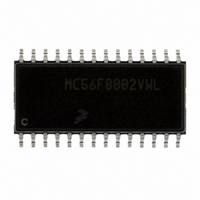
Manufacturer Part Number
MC56F8002VWL
Description
DSC 12K FLASH 32MHZ 28-SOIC
Manufacturer
Freescale Semiconductor
Series
56F8xxxr
Datasheet
1.MC56F8006DEMO.pdf
(100 pages)
Specifications of MC56F8002VWL
Core Processor
56800
Core Size
16-Bit
Speed
32MHz
Connectivity
I²C, LIN, SCI, SPI
Peripherals
LVD, POR, PWM, WDT
Number Of I /o
23
Program Memory Size
12KB (6K x 16)
Program Memory Type
FLASH
Ram Size
1K x 16
Voltage - Supply (vcc/vdd)
1.8 V ~ 3.6 V
Data Converters
A/D 15x12b
Oscillator Type
Internal
Operating Temperature
-40°C ~ 105°C
Package / Case
28-SOIC
Product
DSCs
Data Bus Width
16 bit
Processor Series
MC56F80xx
Core
56800E
Instruction Set Architecture
Dual Harvard
Device Million Instructions Per Second
32 MIPs
Maximum Clock Frequency
32 MHz
Number Of Programmable I/os
40
Data Ram Size
2 KB
Operating Supply Voltage
1.8 V to 3.6 V
Maximum Operating Temperature
+ 105 C
Mounting Style
SMD/SMT
Development Tools By Supplier
MC56F8006DEMO, APMOTOR56F8000E
Interface Type
LIN, I2C, SCI, SPI
Minimum Operating Temperature
- 40 C
For Use With
APMOTOR56F8000E - KIT DEMO MOTOR CTRL SYSTEM
Lead Free Status / RoHS Status
Lead free / RoHS Compliant
Eeprom Size
-
Lead Free Status / Rohs Status
Lead free / RoHS Compliant
Available stocks
Company
Part Number
Manufacturer
Quantity
Price

Part Number:
MC56F8002VWL
Manufacturer:
FREESCALE
Quantity:
20 000


Overview
6
•
•
•
•
•
— Double-buffered PWM registers
— Separate deadtime insertions for rising and falling edges
— Separate top and bottom pulse-width correction by means of software
— Asymmetric PWM output within both Center Aligned and Edge Aligned operation
— Separate top and bottom polarity control
— Each complementary PWM signal pair allows selection of a PWM supply source from:
Two independent 12-bit analog-to-digital converters (ADCs)
— 2 x 14 channel external inputs plus seven internal inputs
— Support simultaneous and software triggering conversions
— ADC conversions can be synchronized by PWM and PDB modules
— Sampling rate up to 400 KSPS for 10- or 12-bit conversion result; 470 KSPS for 8-bit conversion result
— Two 16-word result registers
Two programmable gain amplifier (PGAs)
— Each PGA is designed to amplify and convert differential signals to a single-ended value fed to one of the ADC
— 1X, 2X, 4X, 8X, 16X, or 32X gain
— Software and hardware triggers are available
— Integrated sample/hold circuit
— Includes additional calibration features:
Three analog comparators (CMPs)
— Selectable input source includes external pins, internal DACs
— Programmable output polarity
— Output can drive timer input, PWM fault input, PWM source, external pin output, and trigger ADCs
— Output falling and rising edge detection able to generate interrupts
One dual channel 16-bit multi-purpose timer module (TMR)
— Two independent 16-bit counter/timers with cascading capability
— Up to 96 MHz operating clock
— Each timer has capture and compare and quadrature decoder capability
— Up to 12 operating modes
— Four external inputs and two external outputs
One serial communication interface (SCI) with LIN slave functionality
— Up to 96 MHz operating clock
— Full-duplex or single-wire operation
— Programmable 8- or 9- bit data format
— Two receiver wakeup methods:
— 1/16 bit-time noise detection
– PWM generator
– Internal timers
– Analog comparator outputs
inputs
– Offset calibration eliminates any errors in the internal reference used to generate the VDDA/2 output center
– Gain calibration can be used to verify the gain of the overall datapath
– Both features require software correction of the ADC result
– Idle line
– Address mark
point
MC56F8006/MC56F8002 Digital Signal Controller, Rev. 3
Freescale Semiconductor
Related parts for MC56F8002VWL
Image
Part Number
Description
Manufacturer
Datasheet
Request
R

Part Number:
Description:
Manufacturer:
Freescale Semiconductor, Inc
Datasheet:
Part Number:
Description:
Manufacturer:
Freescale Semiconductor, Inc
Datasheet:
Part Number:
Description:
Manufacturer:
Freescale Semiconductor, Inc
Datasheet:
Part Number:
Description:
Manufacturer:
Freescale Semiconductor, Inc
Datasheet:
Part Number:
Description:
Manufacturer:
Freescale Semiconductor, Inc
Datasheet:
Part Number:
Description:
Manufacturer:
Freescale Semiconductor, Inc
Datasheet:
Part Number:
Description:
Manufacturer:
Freescale Semiconductor, Inc
Datasheet:
Part Number:
Description:
Manufacturer:
Freescale Semiconductor, Inc
Datasheet:
Part Number:
Description:
Manufacturer:
Freescale Semiconductor, Inc
Datasheet:
Part Number:
Description:
Manufacturer:
Freescale Semiconductor, Inc
Datasheet:
Part Number:
Description:
Manufacturer:
Freescale Semiconductor, Inc
Datasheet:
Part Number:
Description:
Manufacturer:
Freescale Semiconductor, Inc
Datasheet:
Part Number:
Description:
Manufacturer:
Freescale Semiconductor, Inc
Datasheet:
Part Number:
Description:
Manufacturer:
Freescale Semiconductor, Inc
Datasheet:
Part Number:
Description:
Manufacturer:
Freescale Semiconductor, Inc
Datasheet: