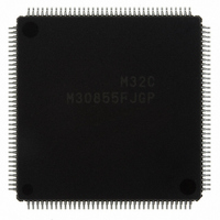
M30855FJGP#U3 Renesas Electronics America, M30855FJGP#U3 Datasheet - Page 367

M30855FJGP#U3
Manufacturer Part Number
M30855FJGP#U3
Description
IC M32C MCU FLASH 512K 144LQFP
Manufacturer
Renesas Electronics America
Series
M16C™ M32C/80r
Specifications of M30855FJGP#U3
Core Processor
M32C/80
Core Size
16/32-Bit
Speed
32MHz
Connectivity
CAN, I²C, IEBus, SIO, UART/USART
Peripherals
DMA, WDT
Number Of I /o
121
Program Memory Size
512KB (512K x 8)
Program Memory Type
FLASH
Ram Size
24K x 8
Voltage - Supply (vcc/vdd)
3 V ~ 5.5 V
Data Converters
A/D 34x10b, D/A 2x8b
Oscillator Type
Internal
Operating Temperature
-40°C ~ 85°C
Package / Case
144-LQFP
For Use With
R0K330879S001BE - KIT DEV RSK M32C/87R0K330879S000BE - KIT DEV RSK M32C/87
Lead Free Status / RoHS Status
Lead free / RoHS Compliant
Eeprom Size
-
Available stocks
Company
Part Number
Manufacturer
Quantity
Price
- Current page: 367 of 544
- Download datasheet (4Mb)
M
R
R
e
E
3
. v
J
2
Figure 23.18 C0MDR and C1MDR Registers
0
C
23.1.16 CANi Mode Register (CiMDR Register)
1
9
0 .
8 /
B
0
3
23.1.16.1 CMOD Bit
5
The CMOD bit selects a CAN operating mode.
0
• Normal operating mode: The CAN module transmits and receives data as expected.
• Bus monitoring mode
• Self-test mode: The CAN module connects the CANi
3
G
J
NOTES:
7
u
o r
0 -
. l
CANi Mode Register
b7
1. Do not generate a transmit request in bus monitoring mode.
u
0
1
NOTES:
p
, 1
0
The CAN module assumes the ACK bit is set to dominant "L" regardless of the ACK bit setting.
Therefore, when the CRC delimiter is received as expected, the CAN module determines the
data is received with no error regardless of the ACK bit setting.
b6
3
(
1. Set the CiMDR register when the STATE_RESET bit in the CiSTR register is set to "1" (CAN module
2. Value is obtained by setting the SLEEP bit in the CiSLPR register to "1" (sleep mode exited) after
2
M
0
b5
reset completed).
reset and supplying the clock to the CAN module.
3
0
2
5
b4
C
8 /
Page 342
b3
, 5
Output signal from the CANi
transmitting data. Figure 23.19 shows an image diagram in self-test mode.
The CAN module can communicate without additional device in loop back mode.
b2
M
3
b1
2
C
(1)
b0
f o
8 /
: The CAN module receives data. Output signal from the CANi
4
5
ule transmits neither ACK nor error frame.
fixed as a high-level ("H") signal in bus monitoring mode. The CAN mod
(b7 - b2)
9
Symbol
) T
CMOD
4
Bit
(i=0, 1)
Symbol
C0MDR
C1MDR
CAN Operating Mode
Select Bit
Nothing is assigned. When write, set to "0".
When read, its content is indeterminate.
(1)
Bit Name
Address
0219
0299
OUT
16
16
pin is fixed as an "H" signal in self-test mode while
(i=0, 1)
OUT
b1 b0
0 0: Normal operating mode
0 1: Bus monitoring mode
1 0: Self-test mode
1 1: Do not set to this value
pin to the CANi
After Reset
XXXX XX00
XXXX XX00
Function
IN
(2)
2
2
pin internally.
23. CAN Module
RW
RW
RW
OUT
pin is
Related parts for M30855FJGP#U3
Image
Part Number
Description
Manufacturer
Datasheet
Request
R

Part Number:
Description:
KIT STARTER FOR M16C/29
Manufacturer:
Renesas Electronics America
Datasheet:

Part Number:
Description:
KIT STARTER FOR R8C/2D
Manufacturer:
Renesas Electronics America
Datasheet:

Part Number:
Description:
R0K33062P STARTER KIT
Manufacturer:
Renesas Electronics America
Datasheet:

Part Number:
Description:
KIT STARTER FOR R8C/23 E8A
Manufacturer:
Renesas Electronics America
Datasheet:

Part Number:
Description:
KIT STARTER FOR R8C/25
Manufacturer:
Renesas Electronics America
Datasheet:

Part Number:
Description:
KIT STARTER H8S2456 SHARPE DSPLY
Manufacturer:
Renesas Electronics America
Datasheet:

Part Number:
Description:
KIT STARTER FOR R8C38C
Manufacturer:
Renesas Electronics America
Datasheet:

Part Number:
Description:
KIT STARTER FOR R8C35C
Manufacturer:
Renesas Electronics America
Datasheet:

Part Number:
Description:
KIT STARTER FOR R8CL3AC+LCD APPS
Manufacturer:
Renesas Electronics America
Datasheet:

Part Number:
Description:
KIT STARTER FOR RX610
Manufacturer:
Renesas Electronics America
Datasheet:

Part Number:
Description:
KIT STARTER FOR R32C/118
Manufacturer:
Renesas Electronics America
Datasheet:

Part Number:
Description:
KIT DEV RSK-R8C/26-29
Manufacturer:
Renesas Electronics America
Datasheet:

Part Number:
Description:
KIT STARTER FOR SH7124
Manufacturer:
Renesas Electronics America
Datasheet:

Part Number:
Description:
KIT STARTER FOR H8SX/1622
Manufacturer:
Renesas Electronics America
Datasheet:

Part Number:
Description:
KIT DEV FOR SH7203
Manufacturer:
Renesas Electronics America
Datasheet:


