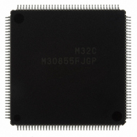
M30855FJGP#U3 Renesas Electronics America, M30855FJGP#U3 Datasheet - Page 391

M30855FJGP#U3
Manufacturer Part Number
M30855FJGP#U3
Description
IC M32C MCU FLASH 512K 144LQFP
Manufacturer
Renesas Electronics America
Series
M16C™ M32C/80r
Specifications of M30855FJGP#U3
Core Processor
M32C/80
Core Size
16/32-Bit
Speed
32MHz
Connectivity
CAN, I²C, IEBus, SIO, UART/USART
Peripherals
DMA, WDT
Number Of I /o
121
Program Memory Size
512KB (512K x 8)
Program Memory Type
FLASH
Ram Size
24K x 8
Voltage - Supply (vcc/vdd)
3 V ~ 5.5 V
Data Converters
A/D 34x10b, D/A 2x8b
Oscillator Type
Internal
Operating Temperature
-40°C ~ 85°C
Package / Case
144-LQFP
For Use With
R0K330879S001BE - KIT DEV RSK M32C/87R0K330879S000BE - KIT DEV RSK M32C/87
Lead Free Status / RoHS Status
Lead free / RoHS Compliant
Eeprom Size
-
Available stocks
Company
Part Number
Manufacturer
Quantity
Price
- Current page: 391 of 544
- Download datasheet (4Mb)
M
R
R
23.4 CAN Interrupts
e
E
3
. v
J
2
Figure 23.40 Operation Timing when CAN Bus Error Occurs
0
C
23.3.4 CAN Bus Error Timing
The CAN1 wake-up interrupt and CANij interrupts (i=0,1,j=0 to 2) are provided as the CAN interrupt.
23.4.1 CAN1 Wake-Up Interrupt
23.4.2 CANij Interrupts
1
9
0 .
8 /
B
Figure 23.40 shows an operation example of when a CAN bus error occurs.
When a signal applied to the CAN1WU pin is on the falling edge, the CAN1WUR bit in the IIO5IR register
is set to "1" (interrupt requested). At this time, the IR bit in the CAN5IC register is set to "1" (interrupt
requested) if the CAN1WUE bit in the IIO5IE register is set to "1" (interrupt enabled).
If P7
counter mode of Timer A3 (TA3
If P8
available by using INT1 that shares a pin with CAN0
Figure 23.41 shows a block diagram of the CANij interrupts. The followings cause the CAN-associated
interrupt request to be generated.
The INTSEL bit in the CiCTLR1 register determines how an interrupt request is generated. When the
INTSEL bit is set to "0", one of the above CANi interrupt request source causes the CANij interrupts to
be generated by the OR circuit. When the INTSEL bit is set to "1", CANi transmission completed, CANi
reception completed and CANi errors (CANi bus error detection, CANi module into error-passive state
and CANi module into bus-off state) cause the CANij interrupt corresponding to each source to be
generated.
- The CANi slot k (k=0 to 15) completes a transmission
- The CANi slot k completes a reception
- The CANi module detects a bus error
- The CANi module moves into an error-passive state
- The CANi module moves into a bus-off state
0
3
5
0
(1) When a CAN bus error is detected, the STATE_BUSERROR bit in the CiSTR register is set to "1",
3
G
J
7
u
7
3
o r
0 -
. l
(error occurred) and the BEIS bit in the CiEISTR register is set to "1" (interrupt requested). The
CAN starts transmitting the error frame.
(CAN0
(CAN0
u
0
1
p
, 1
0
3
(
2
M
0
BEIS bit
CAN bus
STATE_BUSERROR
bit
3
0
IN
IN
2
5
) is used as a CAN0 input port, the CAN0 wake-up interrupt is available by using event
C
/CAN1
8 /
Page 366
, 5
________
M
IN
3
2
) is used as a CAN input port, the CAN0 and CAN1 wake-up interrupts are
C
f o
8 /
_______________
4
5
9
) T
4
IN
) that shares a pin with CAN0.
"1"
"1"
"0"
"0"
Transmit / receive frame
IN
/CAN1
(1)
IN
.
Error detected
Error frame
23. CAN Module
Related parts for M30855FJGP#U3
Image
Part Number
Description
Manufacturer
Datasheet
Request
R

Part Number:
Description:
KIT STARTER FOR M16C/29
Manufacturer:
Renesas Electronics America
Datasheet:

Part Number:
Description:
KIT STARTER FOR R8C/2D
Manufacturer:
Renesas Electronics America
Datasheet:

Part Number:
Description:
R0K33062P STARTER KIT
Manufacturer:
Renesas Electronics America
Datasheet:

Part Number:
Description:
KIT STARTER FOR R8C/23 E8A
Manufacturer:
Renesas Electronics America
Datasheet:

Part Number:
Description:
KIT STARTER FOR R8C/25
Manufacturer:
Renesas Electronics America
Datasheet:

Part Number:
Description:
KIT STARTER H8S2456 SHARPE DSPLY
Manufacturer:
Renesas Electronics America
Datasheet:

Part Number:
Description:
KIT STARTER FOR R8C38C
Manufacturer:
Renesas Electronics America
Datasheet:

Part Number:
Description:
KIT STARTER FOR R8C35C
Manufacturer:
Renesas Electronics America
Datasheet:

Part Number:
Description:
KIT STARTER FOR R8CL3AC+LCD APPS
Manufacturer:
Renesas Electronics America
Datasheet:

Part Number:
Description:
KIT STARTER FOR RX610
Manufacturer:
Renesas Electronics America
Datasheet:

Part Number:
Description:
KIT STARTER FOR R32C/118
Manufacturer:
Renesas Electronics America
Datasheet:

Part Number:
Description:
KIT DEV RSK-R8C/26-29
Manufacturer:
Renesas Electronics America
Datasheet:

Part Number:
Description:
KIT STARTER FOR SH7124
Manufacturer:
Renesas Electronics America
Datasheet:

Part Number:
Description:
KIT STARTER FOR H8SX/1622
Manufacturer:
Renesas Electronics America
Datasheet:

Part Number:
Description:
KIT DEV FOR SH7203
Manufacturer:
Renesas Electronics America
Datasheet:


