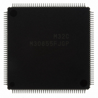
M30855FJGP#U3 Renesas Electronics America, M30855FJGP#U3 Datasheet - Page 534

M30855FJGP#U3
Manufacturer Part Number
M30855FJGP#U3
Description
IC M32C MCU FLASH 512K 144LQFP
Manufacturer
Renesas Electronics America
Series
M16C™ M32C/80r
Specifications of M30855FJGP#U3
Core Processor
M32C/80
Core Size
16/32-Bit
Speed
32MHz
Connectivity
CAN, I²C, IEBus, SIO, UART/USART
Peripherals
DMA, WDT
Number Of I /o
121
Program Memory Size
512KB (512K x 8)
Program Memory Type
FLASH
Ram Size
24K x 8
Voltage - Supply (vcc/vdd)
3 V ~ 5.5 V
Data Converters
A/D 34x10b, D/A 2x8b
Oscillator Type
Internal
Operating Temperature
-40°C ~ 85°C
Package / Case
144-LQFP
For Use With
R0K330879S001BE - KIT DEV RSK M32C/87R0K330879S000BE - KIT DEV RSK M32C/87
Lead Free Status / RoHS Status
Lead free / RoHS Compliant
Eeprom Size
-
Available stocks
Company
Part Number
Manufacturer
Quantity
Price
- Current page: 534 of 544
- Download datasheet (4Mb)
Rev.
REVISION HISTORY
Date
252-258
Page
158
185
189
190
193
195
196
197
208
211
219
230
245
246
247
248
261
275
277
280
281
285
288
289
• Figure 15.7 TRGSR Register and TCSPR Register Added note 2 to the
Three-Phase Motor Control Timer Functions
• Figure 16.4 DM0SL to DM3SLRegister Value after reset changed
• Figure 16.8 Triangular Wave Modulation Operation Figure modified
• Figure 16.9 Sawtooth Wave Modulation Operation Figure modified
Serial I/O
• Figure 17.2 U0TB to U4TB Registers and U0RB to U4RB Registers Note 3
• Figure 17.4 U0C0 to U4C0 Registers Note 3 added
• Figure 17.5 U0C1 to U4C1 Registers and U0SMR to U4SMR Registers Note
• Figure 17.6 U0SMR2 to U4SMR2 Registers Reference on note 1 changed
• Table 17.7 Registers to be Used and Settings in UART UiLCH bit function
• Figure 17.15 Receive Operation Figure modified
• Table 17.11 Transfer Speed added
• Figures 17.15 to 17.17 Pin Settings in I
• Table 17.16 Pin Settings (3) PSC3 reigster added
• Table17.24 GCI Mode Specifications Transmit/receive start condition modified
A/D Converter
• Table 18.1 A/D Converter Specifications Note 2 modified; note 3 added
• Figure 18.1 A/D Converter Block Diagram modified
• Figure 18.2 AD0CON0 Register Note 5 modified; notes 8 and 9 added
• Figure 18.3 AD0CON1 Register Notes 10 and 11 added
• Tables 18.2 to 18.8 Each mode specification Note 1 added
• 18.2.8 Output Impedance of Sensor at A/D Conversion added
• Figure 18.8 Analog Input Pin and External Sensor Equivalent Circuit Value
Intelligent I/O
• Figure 22.4 G1BCR1 Register RST2 bit function changed
• Figure 22.6 G1TM0 to G1TM7 Registers and G1POCR0 to G1POCR7 Registers
• Table 22.2 Base Timer Specifications Base timer reset condition modified
• Figure 22.9 Base Timer Block Diagram Block diagram modified
• Table 22.4 Time Measurement Function Specifications Description for the
• Figure 22.14 Time Measurement Function (2) Figure modified
• Figure 22.15 Prescaler Function and Gate Function Item modified
TCSPR register
for the U0RB to U4RB registers modified
2 for the U0C1 to U4C1 registers added
modified
for the condenser changed
Notes 6 and 7 added to the G1POCR0 to G1POCR7 registers
gate function modified
M32C/85 Group(M32C/85, M32C/85T) Hardware Manual
C-15
Description
Summary
2
C Mode Input settings added to tables
Related parts for M30855FJGP#U3
Image
Part Number
Description
Manufacturer
Datasheet
Request
R

Part Number:
Description:
KIT STARTER FOR M16C/29
Manufacturer:
Renesas Electronics America
Datasheet:

Part Number:
Description:
KIT STARTER FOR R8C/2D
Manufacturer:
Renesas Electronics America
Datasheet:

Part Number:
Description:
R0K33062P STARTER KIT
Manufacturer:
Renesas Electronics America
Datasheet:

Part Number:
Description:
KIT STARTER FOR R8C/23 E8A
Manufacturer:
Renesas Electronics America
Datasheet:

Part Number:
Description:
KIT STARTER FOR R8C/25
Manufacturer:
Renesas Electronics America
Datasheet:

Part Number:
Description:
KIT STARTER H8S2456 SHARPE DSPLY
Manufacturer:
Renesas Electronics America
Datasheet:

Part Number:
Description:
KIT STARTER FOR R8C38C
Manufacturer:
Renesas Electronics America
Datasheet:

Part Number:
Description:
KIT STARTER FOR R8C35C
Manufacturer:
Renesas Electronics America
Datasheet:

Part Number:
Description:
KIT STARTER FOR R8CL3AC+LCD APPS
Manufacturer:
Renesas Electronics America
Datasheet:

Part Number:
Description:
KIT STARTER FOR RX610
Manufacturer:
Renesas Electronics America
Datasheet:

Part Number:
Description:
KIT STARTER FOR R32C/118
Manufacturer:
Renesas Electronics America
Datasheet:

Part Number:
Description:
KIT DEV RSK-R8C/26-29
Manufacturer:
Renesas Electronics America
Datasheet:

Part Number:
Description:
KIT STARTER FOR SH7124
Manufacturer:
Renesas Electronics America
Datasheet:

Part Number:
Description:
KIT STARTER FOR H8SX/1622
Manufacturer:
Renesas Electronics America
Datasheet:

Part Number:
Description:
KIT DEV FOR SH7203
Manufacturer:
Renesas Electronics America
Datasheet:


