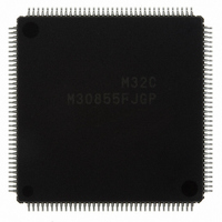
M30855FJGP#U3 Renesas Electronics America, M30855FJGP#U3 Datasheet - Page 378

M30855FJGP#U3
Manufacturer Part Number
M30855FJGP#U3
Description
IC M32C MCU FLASH 512K 144LQFP
Manufacturer
Renesas Electronics America
Series
M16C™ M32C/80r
Specifications of M30855FJGP#U3
Core Processor
M32C/80
Core Size
16/32-Bit
Speed
32MHz
Connectivity
CAN, I²C, IEBus, SIO, UART/USART
Peripherals
DMA, WDT
Number Of I /o
121
Program Memory Size
512KB (512K x 8)
Program Memory Type
FLASH
Ram Size
24K x 8
Voltage - Supply (vcc/vdd)
3 V ~ 5.5 V
Data Converters
A/D 34x10b, D/A 2x8b
Oscillator Type
Internal
Operating Temperature
-40°C ~ 85°C
Package / Case
144-LQFP
For Use With
R0K330879S001BE - KIT DEV RSK M32C/87R0K330879S000BE - KIT DEV RSK M32C/87
Lead Free Status / RoHS Status
Lead free / RoHS Compliant
Eeprom Size
-
Available stocks
Company
Part Number
Manufacturer
Quantity
Price
- Current page: 378 of 544
- Download datasheet (4Mb)
M
R
R
e
E
3
. v
J
2
Figure 23.29 C0MCTL0 to C0MCTL15 Registers and C1MCTL0 to C1MCTL15 Registers
0
C
23.1.20 CANi Message Slot j Control Register (CiMCTLj Register)
1
9
8 /
0 .
B
0
3
5
0
G
3
J
7
u
o r
0 -
. l
CANi Message Slot j Control Register
u
b7
0
1
p
NOTES:
, 1
0
3
b6
(
3. The C0MCTL0 to C0MCTL4 registers each share addresses with the C0LMAR0 to C0LMAR4
4. The C0MCTL8 to C0MCTL12 registers each share addresses with the C0LMBR0 to C0LMBR4
5. The C1MCTL0 to C1MCTL4 registers each share addresses with the C1LMAR0 to C1LMAR4
6. The C1MCTL8 to C1MCTL12 registers each share addresses with the C1LMBR0 to C1LMBR4
7. Set to "0" by program. If it is set to "1", the value before setting to "1" remains.
2
1. The CiMCTLj register can be accessed only when the BANKSEL bit in the CiCTLR1 register is set to
2. Value is obtained by setting the SLEEP bit in the CiSLPR register to "1" (sleep mode exited) after
M
0
registers.
registers.
3
b5
registers.
registers.
"0" (message slot control register and single-shot register selected).
reset, supplying the clock to the CAN module, and setting the BANKSEL bit to "0".
0
2
5
C
b4
8 /
Page 353
b3
, 5
b2
M
3
b1
2
C
f o
b0
8 /
RSPLOCK
4
5
TRMREQ
When transmit,
When transmit,
MSGLOST
REMOTE
RECREQ
REMACTIVE
When receive,
When receive,
TRMACTIVE
9
SENTDATA
INVALDATA
Symbol
) T
NEWDATA
Symbol
C0MCTL0 to C0MCTL3
C0MCTL4 to C0MCTL7
C0MCTL8 to C0MCTL11
C0MCTL12 to C0MCTL15
C1MCTL0 to C1MCTL3
C1MCTL4 to C1MCTL7
C1MCTL8 to C1MCTL11
C1MCTL12 to C1MCTL15
4
Bit
Receive Complete
Flag
Transmit Complete
Flag
Receiving Flag
Transmitting Flag
Automatic
Answering
Disable Mode
Select Bit
Remote Frame
Set Bit
Receive
Request Bit
Transmit
Request Bit
Overwrite Flag
Remote Frame
Transmit/Receive
Status Flag
Bit Name
(7)
Address
0230
0234
0238
023C
02B0
02B4
02B8
02BC
When transmitting
0: Not transmitted
1: Transmit complete
When transmitting
0: Except transmitting
1: Transmittting
0: No overrun error occurs
1: Overrun error occurs
In modes other than BasicCan mode
0: Data frame
1: Remote frame
In BasicCan mode
0: Receives the data frame (status)
1: Receives the remote frame (status)
0: Enables automatic answering of the remote
1: Disables automatic answering of the remote
0: Transmits/receives the data frame
1: Transmits/receives the remote frame
0: No request to receive the frame
1: Request to receive the frame
0: No request to transmit the frame
1: Request to transmit the frame
frame
frame
(i=0,1, j=0 to 15)
16
16
16
16
16
16
16
16
(3)
(3)
(4)
(4)
(5)
(5)
(6)
(6)
,
,
,
,
,
,
,
,
0231
0235
0239
02B1
02B5
02B9
023D
02BD
16
16,
16
16
16,
16
16,
16,
(3)
(4)
(5)
(6)
0236
02B6
,
,
023E
02BE
,
,
0232
023A
02B2
02BA
Function
(4)
16,
16,
16,
(1)
16
16,
16
16
16
0237
(3)
02B7
023F
(4)
(5)
02BF
(6)
,
,
When receiving
0: Not received
1: Receive complete
When receiving
0: Except storing
1: Stores received data
,
0233
,
023B
02B3
02BB
16
received data
16
16
16
16
16
16
16
(3)
(4)
(5)
(6)
After Reset
00
00
00
00
00
00
00
00
16
16
16
16
16
16
16
16
(i=0,1, j=0 to 15)
(4)
(2)
RW
RW
RW
RW
RW
RW
RW
RO
RO
23. CAN Module
Related parts for M30855FJGP#U3
Image
Part Number
Description
Manufacturer
Datasheet
Request
R

Part Number:
Description:
KIT STARTER FOR M16C/29
Manufacturer:
Renesas Electronics America
Datasheet:

Part Number:
Description:
KIT STARTER FOR R8C/2D
Manufacturer:
Renesas Electronics America
Datasheet:

Part Number:
Description:
R0K33062P STARTER KIT
Manufacturer:
Renesas Electronics America
Datasheet:

Part Number:
Description:
KIT STARTER FOR R8C/23 E8A
Manufacturer:
Renesas Electronics America
Datasheet:

Part Number:
Description:
KIT STARTER FOR R8C/25
Manufacturer:
Renesas Electronics America
Datasheet:

Part Number:
Description:
KIT STARTER H8S2456 SHARPE DSPLY
Manufacturer:
Renesas Electronics America
Datasheet:

Part Number:
Description:
KIT STARTER FOR R8C38C
Manufacturer:
Renesas Electronics America
Datasheet:

Part Number:
Description:
KIT STARTER FOR R8C35C
Manufacturer:
Renesas Electronics America
Datasheet:

Part Number:
Description:
KIT STARTER FOR R8CL3AC+LCD APPS
Manufacturer:
Renesas Electronics America
Datasheet:

Part Number:
Description:
KIT STARTER FOR RX610
Manufacturer:
Renesas Electronics America
Datasheet:

Part Number:
Description:
KIT STARTER FOR R32C/118
Manufacturer:
Renesas Electronics America
Datasheet:

Part Number:
Description:
KIT DEV RSK-R8C/26-29
Manufacturer:
Renesas Electronics America
Datasheet:

Part Number:
Description:
KIT STARTER FOR SH7124
Manufacturer:
Renesas Electronics America
Datasheet:

Part Number:
Description:
KIT STARTER FOR H8SX/1622
Manufacturer:
Renesas Electronics America
Datasheet:

Part Number:
Description:
KIT DEV FOR SH7203
Manufacturer:
Renesas Electronics America
Datasheet:


