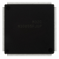
M30855FJGP#U3 Renesas Electronics America, M30855FJGP#U3 Datasheet - Page 536

M30855FJGP#U3
Manufacturer Part Number
M30855FJGP#U3
Description
IC M32C MCU FLASH 512K 144LQFP
Manufacturer
Renesas Electronics America
Series
M16C™ M32C/80r
Specifications of M30855FJGP#U3
Core Processor
M32C/80
Core Size
16/32-Bit
Speed
32MHz
Connectivity
CAN, I²C, IEBus, SIO, UART/USART
Peripherals
DMA, WDT
Number Of I /o
121
Program Memory Size
512KB (512K x 8)
Program Memory Type
FLASH
Ram Size
24K x 8
Voltage - Supply (vcc/vdd)
3 V ~ 5.5 V
Data Converters
A/D 34x10b, D/A 2x8b
Oscillator Type
Internal
Operating Temperature
-40°C ~ 85°C
Package / Case
144-LQFP
For Use With
R0K330879S001BE - KIT DEV RSK M32C/87R0K330879S000BE - KIT DEV RSK M32C/87
Lead Free Status / RoHS Status
Lead free / RoHS Compliant
Eeprom Size
-
Available stocks
Company
Part Number
Manufacturer
Quantity
Price
- Current page: 536 of 544
- Download datasheet (4Mb)
Rev.
REVISION HISTORY
Date
414 - 416
417, 418
Page
384
385
385
386
387
388
390
392
393
451
421
422
426
428
433
434
438
426
445
446
447
449
462
463
-
• Figure 24.18 IPSA Register Bit name and function for the IPSA_0 bit changed
• Table 24.1 Unassigned Pin Setting in Single-Chip Mode Notes modified
• Table 24.2 Unassigned Pin Setting in Memory Expansion Mode and Micro-
• Figure 24.19 Unassigned Pin Handling Figure modified
• Table 24.3 Port P6 Peripheral Function Output Control Bits 3, 6 and 7 modified
• Table 24.4 Port P7 Peripheral Function Output Control Bits 0 and 1 modified
• Table 24.6 Port P9 Peripheral Function Output Control Bits 2 and 6 modified
Flash Memory Version
• Table 25.1 Flash Memory Version Specificatins Item modified
• 25.2.1 ROM Code Protect Function Description modified
• Figure 25.2 ROMCP Register Bits 4 and 5 deleted; notes 2, 3 and 4 modified
• Figures 25.14 to 25.16 Pin Connections in Standard Serial I/O Mode Figures
• Figure 25.19 Circuit Application in Standard Serial I/O Mode Figures modified
Electrical Characteristics
• 26.2 Electrical Characteristics (M32C/85T) Newly added
• Table 26.2 Recommended Operating Conditions (1) f
• Table 26.2 Recommended Operating Conditions (2) Condition and Standard
• Table 26.3 Electrical Characteristics Standard value of V
• Table 26.6 Flash Memory Electrical Characteristics Notes modified
• Table 26.22 Memory Expansion Mode and Microprocessor Mode Note 3
• Table 26.23 Memory Expansion Mode and Microprocessor Mode Note 5
• Figure 26.5 V
• Table 26.24 Electrical Characteristics Standard value of V
• Table 26.40 Memory Expansion Mode and Microprocessor Mode Note 3 added
• Table 26.41 Memory Expansion Mode and Microprocessor Mode Note 5 added
• Figure 26.7 V
• Figure 26.9 V
Precautions
• Section of Processor Mode delected
• 27.1 Restrictions to Use M32C/85T (High-Reliability Version) Newly added
• 27.2 Reset added
processor Mode Table modified; notes modified
modified
SV
value of f
dard value of I
power consumption mode added
added
added
CC
and note 1 added
(Ring)
M32C/85 Group(M32C/85, M32C/85T) Hardware Manual
CC1
CC1
CC1
added
CC
=V
, when f
=V
=V
CC2
CC2
CC2
C-17
=3.3V Timing (1) Formula of th
=5V Timing (3) NMI input added
=3.3V Timing (3) NMI input added
(BCLK)
Description
=32MHz, modifed standard value of I
Summary
_______
_______
(WR-DB)
(ripple)
OH
OH
on note 3 modified
, Vp-p
modified; stan-
modified
(ripple)
CC
, V
in low
CC
,
Related parts for M30855FJGP#U3
Image
Part Number
Description
Manufacturer
Datasheet
Request
R

Part Number:
Description:
KIT STARTER FOR M16C/29
Manufacturer:
Renesas Electronics America
Datasheet:

Part Number:
Description:
KIT STARTER FOR R8C/2D
Manufacturer:
Renesas Electronics America
Datasheet:

Part Number:
Description:
R0K33062P STARTER KIT
Manufacturer:
Renesas Electronics America
Datasheet:

Part Number:
Description:
KIT STARTER FOR R8C/23 E8A
Manufacturer:
Renesas Electronics America
Datasheet:

Part Number:
Description:
KIT STARTER FOR R8C/25
Manufacturer:
Renesas Electronics America
Datasheet:

Part Number:
Description:
KIT STARTER H8S2456 SHARPE DSPLY
Manufacturer:
Renesas Electronics America
Datasheet:

Part Number:
Description:
KIT STARTER FOR R8C38C
Manufacturer:
Renesas Electronics America
Datasheet:

Part Number:
Description:
KIT STARTER FOR R8C35C
Manufacturer:
Renesas Electronics America
Datasheet:

Part Number:
Description:
KIT STARTER FOR R8CL3AC+LCD APPS
Manufacturer:
Renesas Electronics America
Datasheet:

Part Number:
Description:
KIT STARTER FOR RX610
Manufacturer:
Renesas Electronics America
Datasheet:

Part Number:
Description:
KIT STARTER FOR R32C/118
Manufacturer:
Renesas Electronics America
Datasheet:

Part Number:
Description:
KIT DEV RSK-R8C/26-29
Manufacturer:
Renesas Electronics America
Datasheet:

Part Number:
Description:
KIT STARTER FOR SH7124
Manufacturer:
Renesas Electronics America
Datasheet:

Part Number:
Description:
KIT STARTER FOR H8SX/1622
Manufacturer:
Renesas Electronics America
Datasheet:

Part Number:
Description:
KIT DEV FOR SH7203
Manufacturer:
Renesas Electronics America
Datasheet:


