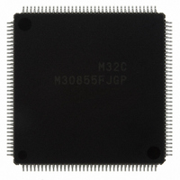
M30855FJGP#U3 Renesas Electronics America, M30855FJGP#U3 Datasheet - Page 523

M30855FJGP#U3
Manufacturer Part Number
M30855FJGP#U3
Description
IC M32C MCU FLASH 512K 144LQFP
Manufacturer
Renesas Electronics America
Series
M16C™ M32C/80r
Specifications of M30855FJGP#U3
Core Processor
M32C/80
Core Size
16/32-Bit
Speed
32MHz
Connectivity
CAN, I²C, IEBus, SIO, UART/USART
Peripherals
DMA, WDT
Number Of I /o
121
Program Memory Size
512KB (512K x 8)
Program Memory Type
FLASH
Ram Size
24K x 8
Voltage - Supply (vcc/vdd)
3 V ~ 5.5 V
Data Converters
A/D 34x10b, D/A 2x8b
Oscillator Type
Internal
Operating Temperature
-40°C ~ 85°C
Package / Case
144-LQFP
For Use With
R0K330879S001BE - KIT DEV RSK M32C/87R0K330879S000BE - KIT DEV RSK M32C/87
Lead Free Status / RoHS Status
Lead free / RoHS Compliant
Eeprom Size
-
Available stocks
Company
Part Number
Manufacturer
Quantity
Price
- Current page: 523 of 544
- Download datasheet (4Mb)
Rev.
REVISION HISTORY
Date
160 - 168 • Figure 14.8, 14.9, 14.12, and 14.13 Value after RESET of the TA0MR to
Page
129
133
134
135
141
142
143
144
147
148
149
151
152
155
157
180
181
182
183
184
185
Watchdog Timer
• 11.1 Count Source Protection Mode modified
DMAC
• Table 12.1 DMAC Specifications CAN Interrupt Request added to DMAC
• Figure 12.2 DM0SL to DM3SL Registers Value after RESET modified; b6 bit
• Table 12.2 DMiSL Register Function Intelligent I/O Interrupt 5 Request
• Table 12.4 Coefficient j, k revised
• Precautions compiled into one chapter, 25. Precautions
DMAC II
• Table 13.1 DMAC II Specifications Note 2 added
• Figure 13.1 RLVL Register Value after RESET modified; Note 3 modified;
• 13.3 Transfer Data modified
• 13.4.2 Burst Transfer modified
• 13.4.4 Chained Transfer modified
Timer
• Figure 14.1 Timer A Configuration modified
• Figure 14.2 Timer B Configuration modified
• Figure 14.5 TA0MR to TA4MR Registers and TABSR Register Value after
• Figure 14.7 TRGSR Register and TCSPR Register Value after RESET of the
Three-Phase Motor Control Timer Functions
• Table 15.2 Pin Settings revised
• Figure 15.1 Three-Phase Motor Control Timer Functions Block Diagram
• Figure 15.2 INVC0 Register revised
• Figure 15.3 INVC1 Register revised
• Figure 15.4 IDB0, IDB1 and DTT Registers Value after RESET of the IDB0
• Figure 15.5 ICTB2 Register, TA1, TA2, TA4, TA11, TA21 and TA41 Registers,
Request Factors
changes to RO reserved bit
changed to CAN5 Interrupt Request; Intelligent I/O Interrupt 11 Request
changed to CAN2 Interrupt Request; Notes 6 and 9 deleted
Note 4 added
RESET of the TA0MR to TA4MR registers modified; b2 bit changed to RW re-
served bit
TRGSR register modified; b4 to b6 bits changed to RO reserved bits
TA4MR registers modified in each mode; b2 changed to RO reserved bit
revised
and IDB1 registers modified; b6 and b7 bits changed to RO reserved bits
and TB2SC Register Note 2 added
M32C/85 Group(M32C/85, M32C/85T) Hardware Manual
C-4
Description
Summary
Related parts for M30855FJGP#U3
Image
Part Number
Description
Manufacturer
Datasheet
Request
R

Part Number:
Description:
KIT STARTER FOR M16C/29
Manufacturer:
Renesas Electronics America
Datasheet:

Part Number:
Description:
KIT STARTER FOR R8C/2D
Manufacturer:
Renesas Electronics America
Datasheet:

Part Number:
Description:
R0K33062P STARTER KIT
Manufacturer:
Renesas Electronics America
Datasheet:

Part Number:
Description:
KIT STARTER FOR R8C/23 E8A
Manufacturer:
Renesas Electronics America
Datasheet:

Part Number:
Description:
KIT STARTER FOR R8C/25
Manufacturer:
Renesas Electronics America
Datasheet:

Part Number:
Description:
KIT STARTER H8S2456 SHARPE DSPLY
Manufacturer:
Renesas Electronics America
Datasheet:

Part Number:
Description:
KIT STARTER FOR R8C38C
Manufacturer:
Renesas Electronics America
Datasheet:

Part Number:
Description:
KIT STARTER FOR R8C35C
Manufacturer:
Renesas Electronics America
Datasheet:

Part Number:
Description:
KIT STARTER FOR R8CL3AC+LCD APPS
Manufacturer:
Renesas Electronics America
Datasheet:

Part Number:
Description:
KIT STARTER FOR RX610
Manufacturer:
Renesas Electronics America
Datasheet:

Part Number:
Description:
KIT STARTER FOR R32C/118
Manufacturer:
Renesas Electronics America
Datasheet:

Part Number:
Description:
KIT DEV RSK-R8C/26-29
Manufacturer:
Renesas Electronics America
Datasheet:

Part Number:
Description:
KIT STARTER FOR SH7124
Manufacturer:
Renesas Electronics America
Datasheet:

Part Number:
Description:
KIT STARTER FOR H8SX/1622
Manufacturer:
Renesas Electronics America
Datasheet:

Part Number:
Description:
KIT DEV FOR SH7203
Manufacturer:
Renesas Electronics America
Datasheet:


