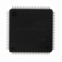
M30833FJGP#U5 Renesas Electronics America, M30833FJGP#U5 Datasheet - Page 324

M30833FJGP#U5
Manufacturer Part Number
M30833FJGP#U5
Description
IC M32C/83 MCU FLASH 100LQFP
Manufacturer
Renesas Electronics America
Series
M16C™ M32C/80r
Datasheets
1.M3087BFLGPU3.pdf
(364 pages)
2.M30833FJGPU3.pdf
(96 pages)
3.M30833FJGPU3.pdf
(529 pages)
Specifications of M30833FJGP#U5
Core Processor
M32C/80
Core Size
16/32-Bit
Speed
32MHz
Connectivity
CAN, I²C, IEBus, SIO, UART/USART
Peripherals
DMA, WDT
Number Of I /o
85
Program Memory Size
512KB (512K x 8)
Program Memory Type
FLASH
Ram Size
31K x 8
Voltage - Supply (vcc/vdd)
3 V ~ 5.5 V
Data Converters
A/D 26x10b; D/A 2x8b
Oscillator Type
Internal
Operating Temperature
-20°C ~ 85°C
Package / Case
100-LQFP
For Use With
R0K330879S001BE - KIT DEV RSK M32C/87R0K330879S000BE - KIT DEV RSK M32C/87
Lead Free Status / RoHS Status
Lead free / RoHS Compliant
Eeprom Size
-
Available stocks
Company
Part Number
Manufacturer
Quantity
Price
Part Number:
M30833FJGP#U5M30833FJGP#U3
Manufacturer:
Renesas Electronics America
Quantity:
10 000
- Current page: 324 of 529
- Download datasheet (5Mb)
R
R
M
e
E
3
. v
J
NOTES:
2
Table 21.22 UART Mode Specifications
0
21.4.2 Clock Asynchronous Serial I/O Mode (UART) (Groups 0 and 1)
Transfer Data Format
Transfer Clock
Transmit Start Condition
Receive Start Condition
Interrupt Request
Error detection
Selectable function
1
C
9
1. The transfer clock must be f
2. Set the GiPOCR2 register and the GiTMCR2 register.
3. When an overrun error occurs, the GiRB register is indeterminate.
3 .
B
In clock asynchronous serial I/O mode (UART), data is transmitted at a desired bit rate and in a desired
transfer data format. Table 21.22 lists specifications of UART mode groups 0 and 1. Table 21.23 lists
registers to be used and their settings. Tables 21.24 to 21.27 list pin settings. Figure 21.40 shows an
example of transmit operation. Figure 21.41 shows an example of receive operation.
8 /
0
1
3
0
3
J
G
4
a
0 -
n
o r
3 .
1
u
, 1
3
p
Item
1
2
(
M
(1, 2)
0
0
3
6
2
C
8 /
Page 299
, 3
M
3
2
• Character Bit (transfer data) :
• Start bit :
• Stop bit :
When the CKDIR bit in the GiMR register (i=0, 1) is set to "0" (internal clock) :
Set the registers associated with the waveform generation function, the GiMR register and
GiERC register. Then, set as written below after at least one transfer clock cycle.
• Set the TE bit in the GiCR register to "1" (transmit enable)
• Set the TI bit in the GiCR register to "0" (data in the GiTB register)
Set the registers associated with the waveform generation function, the GiMR register and
GiERC register. Then, set as written below after at least one transfer clock cycle.
• Set the RE bit in the GiCR register to "1" (receive enable)
• Detect the start bit
• While transmitting, one of the following conditions can be selected to set the SIOiTR
• While receiving, the following condition can be selected to set the SIOiRR bit to "1"
• Overrun error
• Framing Error
• Stop bit length
• LSB first/MSB first
C
f o
bit to "1" (see Figure 10.14):
the GiRB register
n : setting value of the GiPO0 register, 0000
• The GiPO0 register determines the bit rate.
_
_
(see Figure 10.14) :
Data is transferred from the receive register to the GiRB register (data reception is
completed)
This error occurs when the final stop bit of the next data is received before reading
This error occurs when the number of the stop bits set is not detected
The length of the stop bit is selected from 1 bit or 2 bits
Select either bit 0 or bit 7 to transmit/receive data
8 /
4
Transmit clock is generated in phase-delayed waveform output mode of the chan-
nel 3 waveform generation function.
Receive clock is generated with the channel 2 time measurement function.
data is transferred to the transmit register from the GiTB register.
transmit register is completed
The IRS bit in the GiMR register is set to "0" (no data in the GiTB register) and
The IRS bit is set to "1" (transmission completed) and data transfer from the
3
BTi
8
) T
8
divided by six or more.
(3)
21. Intelligent I/O (Group 0, 1 Communication Function)
8 bits long
1 bit long
select length from 1 bit or 2 bits
Specification
16
to FFFF
16
.
2(n+2)
f
BTi
Related parts for M30833FJGP#U5
Image
Part Number
Description
Manufacturer
Datasheet
Request
R

Part Number:
Description:
KIT STARTER FOR M16C/29
Manufacturer:
Renesas Electronics America
Datasheet:

Part Number:
Description:
KIT STARTER FOR R8C/2D
Manufacturer:
Renesas Electronics America
Datasheet:

Part Number:
Description:
R0K33062P STARTER KIT
Manufacturer:
Renesas Electronics America
Datasheet:

Part Number:
Description:
KIT STARTER FOR R8C/23 E8A
Manufacturer:
Renesas Electronics America
Datasheet:

Part Number:
Description:
KIT STARTER FOR R8C/25
Manufacturer:
Renesas Electronics America
Datasheet:

Part Number:
Description:
KIT STARTER H8S2456 SHARPE DSPLY
Manufacturer:
Renesas Electronics America
Datasheet:

Part Number:
Description:
KIT STARTER FOR R8C38C
Manufacturer:
Renesas Electronics America
Datasheet:

Part Number:
Description:
KIT STARTER FOR R8C35C
Manufacturer:
Renesas Electronics America
Datasheet:

Part Number:
Description:
KIT STARTER FOR R8CL3AC+LCD APPS
Manufacturer:
Renesas Electronics America
Datasheet:

Part Number:
Description:
KIT STARTER FOR RX610
Manufacturer:
Renesas Electronics America
Datasheet:

Part Number:
Description:
KIT STARTER FOR R32C/118
Manufacturer:
Renesas Electronics America
Datasheet:

Part Number:
Description:
KIT DEV RSK-R8C/26-29
Manufacturer:
Renesas Electronics America
Datasheet:

Part Number:
Description:
KIT STARTER FOR SH7124
Manufacturer:
Renesas Electronics America
Datasheet:

Part Number:
Description:
KIT STARTER FOR H8SX/1622
Manufacturer:
Renesas Electronics America
Datasheet:

Part Number:
Description:
KIT DEV FOR SH7203
Manufacturer:
Renesas Electronics America
Datasheet:


