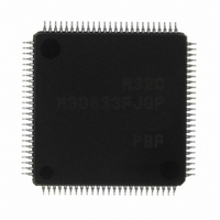
M30833FJGP#U5 Renesas Electronics America, M30833FJGP#U5 Datasheet - Page 406

M30833FJGP#U5
Manufacturer Part Number
M30833FJGP#U5
Description
IC M32C/83 MCU FLASH 100LQFP
Manufacturer
Renesas Electronics America
Series
M16C™ M32C/80r
Datasheets
1.M3087BFLGPU3.pdf
(364 pages)
2.M30833FJGPU3.pdf
(96 pages)
3.M30833FJGPU3.pdf
(529 pages)
Specifications of M30833FJGP#U5
Core Processor
M32C/80
Core Size
16/32-Bit
Speed
32MHz
Connectivity
CAN, I²C, IEBus, SIO, UART/USART
Peripherals
DMA, WDT
Number Of I /o
85
Program Memory Size
512KB (512K x 8)
Program Memory Type
FLASH
Ram Size
31K x 8
Voltage - Supply (vcc/vdd)
3 V ~ 5.5 V
Data Converters
A/D 26x10b; D/A 2x8b
Oscillator Type
Internal
Operating Temperature
-20°C ~ 85°C
Package / Case
100-LQFP
For Use With
R0K330879S001BE - KIT DEV RSK M32C/87R0K330879S000BE - KIT DEV RSK M32C/87
Lead Free Status / RoHS Status
Lead free / RoHS Compliant
Eeprom Size
-
Available stocks
Company
Part Number
Manufacturer
Quantity
Price
Part Number:
M30833FJGP#U5M30833FJGP#U3
Manufacturer:
Renesas Electronics America
Quantity:
10 000
- Current page: 406 of 529
- Download datasheet (5Mb)
R
R
M
e
E
3
. v
J
Figure 24.15 PUR0 Register, PUR1 Register and PUR2 Register
2
0
1
C
9
3 .
B
8 /
0
1
3
0
3
J
G
4
a
0 -
n
o r
3 .
1
u
Pull-Up Control Register 1
Pull-Up Control Register 0
Pull-Up Control Register 2
, 1
3
b7
b7
b7
p
1
2
(
b6
b6
b6
M
0
0
3
b5
b5
b5
6
2
C
NOTES:
NOTES:
NOTES:
b4
b4
b4
Page 381
8 /
1. Set each bit in the PUR1 register to "0" since P0 to P5 operate as the address bus in the
1. Set each bit in the PUR0 register to "0" since P0 to P5 operate as the address bus in the
1. P7
2. P8
, 3
b3
b3
b3
memory expansion mode and microprocessor mode. Pull-up or no pull-up setting can be
selected when using these ports as I/O ports.
memory expansion mode and microprocessor mode. Pull-up or no pull-up setting can be
selected when using these ports as I/O ports.
M
b2
b2
b2
0
5
3
and P7
cannot be pulled up.
b1
b1
b1
2
C
f o
b0
b0
b0
8 /
4
1
3
(b7 - b4)
8
cannot be pulled up.
Symbol
) T
Symbol
Symbol
PU10
PU11
PU12
PU13
8
PU00
PU01
PU02
PU03
PU04
PU05
PU06
PU07
PU20
PU21
PU22
PU23
PU24
PU25
PU26
PU27
Bit
Bit
Bit
Symbol
PUR1
Symbol
PUR0
Symbol
PUR2
P0
P0
P1
P1
P2
P2
P3
P3
P4
P4
P5
P5
P6
P6
P7
P7
P8
P8
P9
P9
Nothing is assigned. When write, set to "0".
When read, its content is indeterminate.
(1)
(1)
0
4
0
4
0
4
0
4
0
4
0
4
0
4
2
4
0
4
0
4
to P0
to P0
to P1
to P1
to P2
to P2
to P3
to P3
to P4
to P4
to P5
to P5
to P6
to P6
to P7
to P7
to P8
to P8
to P9
to P9
Bit Name
Bit Name
Bit Name
3
7
3
7
3
7
3
7
3
7
3
7
3
7
3
7
3
7
3
7
Pull-Up
Pull-Up
Pull-Up
Pull-Up
Pull-Up
Pull-Up
Pull-Up
Pull-Up
Pull-Up
Pull-Up
Pull-Up
Pull-Up
Pull-Up
Pull-Up
Pull-Up
Pull-Up
Pull-Up
Pull-Up
Pull-Up
Pull-Up
Address
03F1
Address
03F0
Address
03DA
16
16
16
(1)
(2)
Pull-up setting for corresponding port
0 : Not pulled up
1 : Pulled up
Pull-up setting for corresponding port
0 : Not pulled up
1 : Pulled up
Pull-up setting for corresponding port
0 : Not pulled up
1 : Pulled up
Function
After Reset
XXXX 0000
After Reset
00
After Reset
00
Function
Function
16
16
2
24. Programmable I/O Port
RW
RW
RW
RW
RW
RW
RW
RW
RW
RW
RW
RW
RW
RW
RW
RW
RW
RW
RW
RW
RW
RW
RW
Related parts for M30833FJGP#U5
Image
Part Number
Description
Manufacturer
Datasheet
Request
R

Part Number:
Description:
KIT STARTER FOR M16C/29
Manufacturer:
Renesas Electronics America
Datasheet:

Part Number:
Description:
KIT STARTER FOR R8C/2D
Manufacturer:
Renesas Electronics America
Datasheet:

Part Number:
Description:
R0K33062P STARTER KIT
Manufacturer:
Renesas Electronics America
Datasheet:

Part Number:
Description:
KIT STARTER FOR R8C/23 E8A
Manufacturer:
Renesas Electronics America
Datasheet:

Part Number:
Description:
KIT STARTER FOR R8C/25
Manufacturer:
Renesas Electronics America
Datasheet:

Part Number:
Description:
KIT STARTER H8S2456 SHARPE DSPLY
Manufacturer:
Renesas Electronics America
Datasheet:

Part Number:
Description:
KIT STARTER FOR R8C38C
Manufacturer:
Renesas Electronics America
Datasheet:

Part Number:
Description:
KIT STARTER FOR R8C35C
Manufacturer:
Renesas Electronics America
Datasheet:

Part Number:
Description:
KIT STARTER FOR R8CL3AC+LCD APPS
Manufacturer:
Renesas Electronics America
Datasheet:

Part Number:
Description:
KIT STARTER FOR RX610
Manufacturer:
Renesas Electronics America
Datasheet:

Part Number:
Description:
KIT STARTER FOR R32C/118
Manufacturer:
Renesas Electronics America
Datasheet:

Part Number:
Description:
KIT DEV RSK-R8C/26-29
Manufacturer:
Renesas Electronics America
Datasheet:

Part Number:
Description:
KIT STARTER FOR SH7124
Manufacturer:
Renesas Electronics America
Datasheet:

Part Number:
Description:
KIT STARTER FOR H8SX/1622
Manufacturer:
Renesas Electronics America
Datasheet:

Part Number:
Description:
KIT DEV FOR SH7203
Manufacturer:
Renesas Electronics America
Datasheet:


