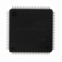
M30833FJGP#U5 Renesas Electronics America, M30833FJGP#U5 Datasheet - Page 386

M30833FJGP#U5
Manufacturer Part Number
M30833FJGP#U5
Description
IC M32C/83 MCU FLASH 100LQFP
Manufacturer
Renesas Electronics America
Series
M16C™ M32C/80r
Datasheets
1.M3087BFLGPU3.pdf
(364 pages)
2.M30833FJGPU3.pdf
(96 pages)
3.M30833FJGPU3.pdf
(529 pages)
Specifications of M30833FJGP#U5
Core Processor
M32C/80
Core Size
16/32-Bit
Speed
32MHz
Connectivity
CAN, I²C, IEBus, SIO, UART/USART
Peripherals
DMA, WDT
Number Of I /o
85
Program Memory Size
512KB (512K x 8)
Program Memory Type
FLASH
Ram Size
31K x 8
Voltage - Supply (vcc/vdd)
3 V ~ 5.5 V
Data Converters
A/D 26x10b; D/A 2x8b
Oscillator Type
Internal
Operating Temperature
-20°C ~ 85°C
Package / Case
100-LQFP
For Use With
R0K330879S001BE - KIT DEV RSK M32C/87R0K330879S000BE - KIT DEV RSK M32C/87
Lead Free Status / RoHS Status
Lead free / RoHS Compliant
Eeprom Size
-
Available stocks
Company
Part Number
Manufacturer
Quantity
Price
Part Number:
M30833FJGP#U5M30833FJGP#U3
Manufacturer:
Renesas Electronics America
Quantity:
10 000
- Current page: 386 of 529
- Download datasheet (5Mb)
R
R
M
23.1 DRAMC Multiplexed Address Output
23.2 Refresh
e
E
3
. v
J
2
0
DRAMC is not available when the PM11 to PM10 bits in the PM1 register are set to "11
PM11 to PM10 bits to "00
the PM02 bit in the PM0 register to "1" (RD/WRH/WRL).
Required wait time between DRAM power-on and memory operation, and necessary processing of dummy
cycle for refresh varies with externally attached DRAM specifications.
DRAMC outputs signals, which are multiplexed row addresses and column addresses, to address bus A
A
23.2.1 Refresh
23.2.2 Self-Refresh
1
C
9
3 .
B
20
Refresh method is the CAS-before-RAS refresh. The REFCNT register controls the refresh interval. Re-
fresh signals are not output in a hold state.
The setting value of the REFCNT register is obtained as follows:
The value of the REFCNT register (00
The refresh signal described in 23.2.1 stops while the CPU stops in stop mode, etc. The DRAM self-
refresh function can be activated by setting the self-refresh before the CPU stops. Setting and cancella-
tion procedures for the self-refresh are as follows:
(1) Setting self-refresh (with 1 wait state, 4 Mbytes)
(2) Cancellation of self-refresh (with 1 wait state, 4M bytes)
Both RAS and CAS are held "L" during self-refresh. When devices other than DRAM are attached, the
______
WR signal is held "L". Take procedures such as applying an "H" signal to the CS.
Figures 23.3 to 23.5 show bus timings during DRAM access.
8 /
0
1
. Figure 23.2 shows an output format for multiplexed addresses.
3
0
3
J
G
4
a
_______
0 -
n
o r
•••
mov.b
mov.b
nop
nop
•••
•••
mov.b
mov.b
mov.b
•••
3 .
1
u
, 1
3
p
1
2
(
M
0
;Execute the nop instruction twice
;
0
3
6
2
#00000001b,DRAMCONT
#10001011b,DRAMCONT
#00000001b,DRAMCONT
#00001011b,DRAMCONT
400h, 400h
_______
C
Page 361
8 /
, 3
M
_______
2
3
," "01
2
C
f o
8 /
4
2
3
8
" or "10
) T
8
_______
16
2
____ ________ ________
" (mode 0 to 2). When the 16-bit DRAM data bus is selected, set
to FF
;Set the AR2 to AR0 bits to "000
;Set the AR2 to AR0 bits again and the SREF bit to "1"
;Set the AR2 to 0 bits to "000
;Set the AR2 to AR0 bits again
;DRAM access is disabled immediately after cancellation.
This is an example of a dummy read operation.
(self-refresh on) simultaneously
and the SREF bit to "0" (DRAM disabled) simultaneously
16
) = refresh interval time / (CPU clock frequency X 32) - 1
2
" (self-refresh cancellation)
2
_____
" (DRAM disabled)
2
" (mode 3). Set the
23. DRAMC
8
to
Related parts for M30833FJGP#U5
Image
Part Number
Description
Manufacturer
Datasheet
Request
R

Part Number:
Description:
KIT STARTER FOR M16C/29
Manufacturer:
Renesas Electronics America
Datasheet:

Part Number:
Description:
KIT STARTER FOR R8C/2D
Manufacturer:
Renesas Electronics America
Datasheet:

Part Number:
Description:
R0K33062P STARTER KIT
Manufacturer:
Renesas Electronics America
Datasheet:

Part Number:
Description:
KIT STARTER FOR R8C/23 E8A
Manufacturer:
Renesas Electronics America
Datasheet:

Part Number:
Description:
KIT STARTER FOR R8C/25
Manufacturer:
Renesas Electronics America
Datasheet:

Part Number:
Description:
KIT STARTER H8S2456 SHARPE DSPLY
Manufacturer:
Renesas Electronics America
Datasheet:

Part Number:
Description:
KIT STARTER FOR R8C38C
Manufacturer:
Renesas Electronics America
Datasheet:

Part Number:
Description:
KIT STARTER FOR R8C35C
Manufacturer:
Renesas Electronics America
Datasheet:

Part Number:
Description:
KIT STARTER FOR R8CL3AC+LCD APPS
Manufacturer:
Renesas Electronics America
Datasheet:

Part Number:
Description:
KIT STARTER FOR RX610
Manufacturer:
Renesas Electronics America
Datasheet:

Part Number:
Description:
KIT STARTER FOR R32C/118
Manufacturer:
Renesas Electronics America
Datasheet:

Part Number:
Description:
KIT DEV RSK-R8C/26-29
Manufacturer:
Renesas Electronics America
Datasheet:

Part Number:
Description:
KIT STARTER FOR SH7124
Manufacturer:
Renesas Electronics America
Datasheet:

Part Number:
Description:
KIT STARTER FOR H8SX/1622
Manufacturer:
Renesas Electronics America
Datasheet:

Part Number:
Description:
KIT DEV FOR SH7203
Manufacturer:
Renesas Electronics America
Datasheet:


