ATTINY24-15MZ Atmel, ATTINY24-15MZ Datasheet - Page 101
ATTINY24-15MZ
Manufacturer Part Number
ATTINY24-15MZ
Description
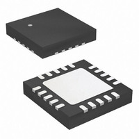
MCU AVR 2K FLASH 15MHZ 20-QFN
Manufacturer
Atmel
Series
AVR® ATtinyr
Datasheet
1.ATTINY24-15MZ.pdf
(225 pages)
Specifications of ATTINY24-15MZ
Package / Case
20-QFN Exposed Pad
Voltage - Supply (vcc/vdd)
2.7 V ~ 5.5 V
Operating Temperature
-40°C ~ 125°C
Speed
16MHz
Number Of I /o
12
Eeprom Size
128 x 8
Core Processor
AVR
Program Memory Type
FLASH
Ram Size
128 x 8
Program Memory Size
2KB (2K x 8)
Data Converters
A/D 8x10b
Oscillator Type
Internal
Peripherals
Brown-out Detect/Reset, POR, PWM, WDT
Connectivity
USI
Core Size
8-Bit
Cpu Family
ATtiny
Device Core
AVR
Device Core Size
8b
Frequency (max)
16MHz
Interface Type
SPI/UART
Total Internal Ram Size
128Byte
# I/os (max)
12
Number Of Timers - General Purpose
2
Operating Supply Voltage (typ)
3.3/5V
Operating Supply Voltage (max)
5.5V
Operating Supply Voltage (min)
2.7V
On-chip Adc
8-chx10-bit
Instruction Set Architecture
RISC
Operating Temp Range
-40C to 125C
Operating Temperature Classification
Automotive
Mounting
Surface Mount
Pin Count
20
Package Type
QFN EP
Lead Free Status / RoHS Status
Lead free / RoHS Compliant


14.8
7701D–AVR–09/10
Compare Match Output Unit
Be aware that the COM1x1:0 bits are not double buffered together with the compare value.
Changing the COM1x1:0 bits will take effect immediately.
The Compare Output mode (COM1x1:0) bits have two functions. The Waveform Generator
uses the COM1x1:0 bits for defining the Output Compare (OC1x) state at the next compare
match. Secondly the COM1x1:0 bits control the OC1x pin output source.
101
registers, I/O bits, and I/O pins in the figure are shown in bold. Only the parts of the general I/O
port control registers (DDR and PORT) that are affected by the COM1x1:0 bits are shown.
When referring to the OC1x state, the reference is for the internal OC1x register, not the OC1x
pin. If a system reset occurs, the OC1x register is reset to "0".
Figure 14-5. Compare Match Output Unit, Schematic
The general I/O port function is overridden by the Output Compare (OC1x) from the Waveform
Generator if either of the COM1x1:0 bits are set. However, the OC1x pin direction (input or
output) is still controlled by the Data Direction Register (DDR) for the port pin. The Data Direc-
tion Register bit for the OC1x pin (DDR_OC1x) must be set as output before the OC1x value is
visible on the pin. The port override function is generally independent of the Waveform Gener-
ation mode, but there are some exceptions. See
112
The design of the Output Compare pin logic allows initialization of the OC1x state before the
output is enabled. Note that some COM1x1:0 bit settings are reserved for certain modes of
operation. See
The COM1x1:0 bits have no effect on the Input Capture unit.
and
shows a simplified schematic of the logic affected by the COM1x1:0 bit settings. The I/O
COMnx1
COMnx0
FOCnx
clk
I/O
Table 14-3 on page 113
“Register Description” on page 112
Waveform
Generator
Atmel ATtiny24/44/84 [Preliminary]
for details.
D
D
D
PORT
DDR
OCnx
Q
Q
Q
Table 14-1 on page
1
0
112,
Figure 14-5 on page
Table 14-2 on page
OCnx
Pin
101
Related parts for ATTINY24-15MZ
Image
Part Number
Description
Manufacturer
Datasheet
Request
R

Part Number:
Description:
Manufacturer:
Atmel Corporation
Datasheet:
Part Number:
Description:
Manufacturer:
Atmel Corporation
Datasheet:

Part Number:
Description:
IC MCU AVR 2K FLASH 20MHZ 20-QFN
Manufacturer:
Atmel
Datasheet:

Part Number:
Description:
IC MCU AVR 2K FLASH 20MHZ 14SOIC
Manufacturer:
Atmel
Datasheet:

Part Number:
Description:
IC MCU AVR 2K FLASH 20MHZ 14-DIP
Manufacturer:
Atmel
Datasheet:

Part Number:
Description:
MCU AVR 2KB FLASH 20MHZ 14SOIC
Manufacturer:
Atmel
Datasheet:
Part Number:
Description:
MCU AVR 2KB FLASH 20MHZ 20QFN
Manufacturer:
Atmel
Datasheet:
Part Number:
Description:
MCU AVR 2K FLASH 15MHZ 14-SOIC
Manufacturer:
Atmel
Datasheet:

Part Number:
Description:
DEV KIT FOR AVR/AVR32
Manufacturer:
Atmel
Datasheet:
Part Number:
Description:
INTERVAL AND WIPE/WASH WIPER CONTROL IC WITH DELAY
Manufacturer:
ATMEL Corporation
Datasheet:
Part Number:
Description:
Low-Voltage Voice-Switched IC for Hands-Free Operation
Manufacturer:
ATMEL Corporation
Datasheet:
Part Number:
Description:
MONOLITHIC INTEGRATED FEATUREPHONE CIRCUIT
Manufacturer:
ATMEL Corporation
Datasheet: