ATTINY24-15MZ Atmel, ATTINY24-15MZ Datasheet - Page 91
ATTINY24-15MZ
Manufacturer Part Number
ATTINY24-15MZ
Description
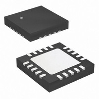
MCU AVR 2K FLASH 15MHZ 20-QFN
Manufacturer
Atmel
Series
AVR® ATtinyr
Datasheet
1.ATTINY24-15MZ.pdf
(225 pages)
Specifications of ATTINY24-15MZ
Package / Case
20-QFN Exposed Pad
Voltage - Supply (vcc/vdd)
2.7 V ~ 5.5 V
Operating Temperature
-40°C ~ 125°C
Speed
16MHz
Number Of I /o
12
Eeprom Size
128 x 8
Core Processor
AVR
Program Memory Type
FLASH
Ram Size
128 x 8
Program Memory Size
2KB (2K x 8)
Data Converters
A/D 8x10b
Oscillator Type
Internal
Peripherals
Brown-out Detect/Reset, POR, PWM, WDT
Connectivity
USI
Core Size
8-Bit
Cpu Family
ATtiny
Device Core
AVR
Device Core Size
8b
Frequency (max)
16MHz
Interface Type
SPI/UART
Total Internal Ram Size
128Byte
# I/os (max)
12
Number Of Timers - General Purpose
2
Operating Supply Voltage (typ)
3.3/5V
Operating Supply Voltage (max)
5.5V
Operating Supply Voltage (min)
2.7V
On-chip Adc
8-chx10-bit
Instruction Set Architecture
RISC
Operating Temp Range
-40C to 125C
Operating Temperature Classification
Automotive
Mounting
Surface Mount
Pin Count
20
Package Type
QFN EP
Lead Free Status / RoHS Status
Lead free / RoHS Compliant


14.2.1
7701D–AVR–09/10
Registers
Figure 14-1. 16-bit Timer/Counter Block Diagram
Note:
The timer/counter (TCNT1), output compare registers (OCR1A/B), and input capture register
(ICR1) are all 16-bit registers. Special procedures must be followed when accessing the 16-bit
registers. These procedures are described in the section
93. The timer/counter control registers (TCCR1A/B) are 8-bit registers, and have no CPU
access restrictions. Interrupt request (abbreviated to Int.Req. in the figure) signals are all visi-
ble in the timer interrupt flag register (TIFR). All interrupts are individually masked with the
timer interrupt mask register (TIMSK). TIFR and TIMSK are not shown in the figure.
The timer/counter can be clocked internally, via the prescaler, or by an external clock source
on the T1 pin. The clock select logic block controls which clock source and edge the
timer/counter uses to increment (or decrement) its value. The timer/counter is inactive when
no clock source is selected. The output from the clock select logic is referred to as the timer
clock (clk
1. See
T
1
).
Figure 1-1 on page 2
Timer/Counter
TCCRnA
OCRnA
OCRnB
TCNTn
ICRn
=
=
Atmel ATtiny24/44/84 [Preliminary]
Direction
Count
Clear
for Timer/Counter1 pin placement and description.
Control Logic
TOP
=
TCCRnB
Values
BOTTOM
Fixed
TOP
ICFn (Int.Req.)
(1)
clk
Detector
Edge
=
Tn
0
“Accessing 16-bit Registers” on page
OCnA
(Int.Req.)
OCnB
(Int.Req.)
TOVn
(Int.Req.)
Clock Select
Generation
Generation
( From Prescaler )
Waveform
Waveform
Canceler
Detector
Noise
Edge
Comparator Ouput )
( From Analog
OCnA
OCnB
ICPn
Tn
91
Related parts for ATTINY24-15MZ
Image
Part Number
Description
Manufacturer
Datasheet
Request
R

Part Number:
Description:
Manufacturer:
Atmel Corporation
Datasheet:
Part Number:
Description:
Manufacturer:
Atmel Corporation
Datasheet:

Part Number:
Description:
IC MCU AVR 2K FLASH 20MHZ 20-QFN
Manufacturer:
Atmel
Datasheet:

Part Number:
Description:
IC MCU AVR 2K FLASH 20MHZ 14SOIC
Manufacturer:
Atmel
Datasheet:

Part Number:
Description:
IC MCU AVR 2K FLASH 20MHZ 14-DIP
Manufacturer:
Atmel
Datasheet:

Part Number:
Description:
MCU AVR 2KB FLASH 20MHZ 14SOIC
Manufacturer:
Atmel
Datasheet:
Part Number:
Description:
MCU AVR 2KB FLASH 20MHZ 20QFN
Manufacturer:
Atmel
Datasheet:
Part Number:
Description:
MCU AVR 2K FLASH 15MHZ 14-SOIC
Manufacturer:
Atmel
Datasheet:

Part Number:
Description:
DEV KIT FOR AVR/AVR32
Manufacturer:
Atmel
Datasheet:
Part Number:
Description:
INTERVAL AND WIPE/WASH WIPER CONTROL IC WITH DELAY
Manufacturer:
ATMEL Corporation
Datasheet:
Part Number:
Description:
Low-Voltage Voice-Switched IC for Hands-Free Operation
Manufacturer:
ATMEL Corporation
Datasheet:
Part Number:
Description:
MONOLITHIC INTEGRATED FEATUREPHONE CIRCUIT
Manufacturer:
ATMEL Corporation
Datasheet: