ATTINY24-15MZ Atmel, ATTINY24-15MZ Datasheet - Page 127
ATTINY24-15MZ
Manufacturer Part Number
ATTINY24-15MZ
Description
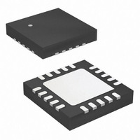
MCU AVR 2K FLASH 15MHZ 20-QFN
Manufacturer
Atmel
Series
AVR® ATtinyr
Datasheet
1.ATTINY24-15MZ.pdf
(225 pages)
Specifications of ATTINY24-15MZ
Package / Case
20-QFN Exposed Pad
Voltage - Supply (vcc/vdd)
2.7 V ~ 5.5 V
Operating Temperature
-40°C ~ 125°C
Speed
16MHz
Number Of I /o
12
Eeprom Size
128 x 8
Core Processor
AVR
Program Memory Type
FLASH
Ram Size
128 x 8
Program Memory Size
2KB (2K x 8)
Data Converters
A/D 8x10b
Oscillator Type
Internal
Peripherals
Brown-out Detect/Reset, POR, PWM, WDT
Connectivity
USI
Core Size
8-Bit
Cpu Family
ATtiny
Device Core
AVR
Device Core Size
8b
Frequency (max)
16MHz
Interface Type
SPI/UART
Total Internal Ram Size
128Byte
# I/os (max)
12
Number Of Timers - General Purpose
2
Operating Supply Voltage (typ)
3.3/5V
Operating Supply Voltage (max)
5.5V
Operating Supply Voltage (min)
2.7V
On-chip Adc
8-chx10-bit
Instruction Set Architecture
RISC
Operating Temp Range
-40C to 125C
Operating Temperature Classification
Automotive
Mounting
Surface Mount
Pin Count
20
Package Type
QFN EP
Lead Free Status / RoHS Status
Lead free / RoHS Compliant


7701D–AVR–09/10
Figure 16-5. Two-wire Mode, Typical Timing Diagram
Referring to the timing diagram
ing steps:
1. The start condition is generated by the Master by forcing the SDA line low while the
2. In addition, the start detector will hold the SCL line low after the master has forced a
3. The Master set the first bit to be transferred and releases the SCL line (C). The Slave
4. After eight bits containing the slave address and data direction (read or write) are
5. If the slave is addressed, it holds the SDA line low during the acknowledgment cycle
6. Multiple bytes can now be transmitted, all in same direction, until a stop condition is
If the slave is not able to receive more data, it does not acknowledge the data byte it has last
received. When the master does a read operation, it must terminate the operation by forcing
the acknowledge bit low after the last byte is transmitted.
Figure 16-6. Start Condition Detector, Logic Diagram
SCL line is high (A). SDA can be forced low either by writing a logical zero to bit 7 of the
shift register, or by setting the corresponding bit in the PORT register to zero. Note that
the data direction register bit must be set to one for the output to be enabled. The slave
device's start detector logic
sets the USISIF Flag. The flag can generate an interrupt if necessary.
negative edge on this line (B). This allows the slave to wake up from sleep or complete
its other tasks before setting up the shift register to receive the address. This is done by
clearing the start condition flag and resetting the counter.
samples the data and shift it into the Serial Register at the positive edge of the SCL
clock.
transferred, the slave counter overflows and the SCL line is forced low (D). If the slave
is not the one the master has addressed, it releases the SCL line and waits for a new
start condition.
before holding the SCL line low again (i.e., the counter register must be set to 14
before releasing SCL at (D)). Depending on the state of the R/W bit, the master or
slave enables its output. If the bit is set, a master read operation is in progress (i.e., the
slave drives the SDA line). The slave can hold the SCL line low after the acknowledge-
ment cycle (E).
given by the master (F), or a new start condition is given.
SDA
SCL
Write( USISIF)
A B
S
C
ADDRESS
SDA
SCL
1 - 7
Atmel ATtiny24/44/84 [Preliminary]
R/W
(Figure 16-5 on page
(Figure 16-6 on page
8
D
ACK
9
E
DATA
1 - 8
D Q
CLR
127) detects the start condition and
127), a bus transfer involves the follow-
ACK
9
D Q
CLR
DATA
1 - 8
USISIF
CLOCK
HOLD
ACK
9
P
F
127
Related parts for ATTINY24-15MZ
Image
Part Number
Description
Manufacturer
Datasheet
Request
R

Part Number:
Description:
Manufacturer:
Atmel Corporation
Datasheet:
Part Number:
Description:
Manufacturer:
Atmel Corporation
Datasheet:

Part Number:
Description:
IC MCU AVR 2K FLASH 20MHZ 20-QFN
Manufacturer:
Atmel
Datasheet:

Part Number:
Description:
IC MCU AVR 2K FLASH 20MHZ 14SOIC
Manufacturer:
Atmel
Datasheet:

Part Number:
Description:
IC MCU AVR 2K FLASH 20MHZ 14-DIP
Manufacturer:
Atmel
Datasheet:

Part Number:
Description:
MCU AVR 2KB FLASH 20MHZ 14SOIC
Manufacturer:
Atmel
Datasheet:
Part Number:
Description:
MCU AVR 2KB FLASH 20MHZ 20QFN
Manufacturer:
Atmel
Datasheet:
Part Number:
Description:
MCU AVR 2K FLASH 15MHZ 14-SOIC
Manufacturer:
Atmel
Datasheet:

Part Number:
Description:
DEV KIT FOR AVR/AVR32
Manufacturer:
Atmel
Datasheet:
Part Number:
Description:
INTERVAL AND WIPE/WASH WIPER CONTROL IC WITH DELAY
Manufacturer:
ATMEL Corporation
Datasheet:
Part Number:
Description:
Low-Voltage Voice-Switched IC for Hands-Free Operation
Manufacturer:
ATMEL Corporation
Datasheet:
Part Number:
Description:
MONOLITHIC INTEGRATED FEATUREPHONE CIRCUIT
Manufacturer:
ATMEL Corporation
Datasheet: