ATTINY24-15MZ Atmel, ATTINY24-15MZ Datasheet - Page 106
ATTINY24-15MZ
Manufacturer Part Number
ATTINY24-15MZ
Description
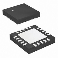
MCU AVR 2K FLASH 15MHZ 20-QFN
Manufacturer
Atmel
Series
AVR® ATtinyr
Datasheet
1.ATTINY24-15MZ.pdf
(225 pages)
Specifications of ATTINY24-15MZ
Package / Case
20-QFN Exposed Pad
Voltage - Supply (vcc/vdd)
2.7 V ~ 5.5 V
Operating Temperature
-40°C ~ 125°C
Speed
16MHz
Number Of I /o
12
Eeprom Size
128 x 8
Core Processor
AVR
Program Memory Type
FLASH
Ram Size
128 x 8
Program Memory Size
2KB (2K x 8)
Data Converters
A/D 8x10b
Oscillator Type
Internal
Peripherals
Brown-out Detect/Reset, POR, PWM, WDT
Connectivity
USI
Core Size
8-Bit
Cpu Family
ATtiny
Device Core
AVR
Device Core Size
8b
Frequency (max)
16MHz
Interface Type
SPI/UART
Total Internal Ram Size
128Byte
# I/os (max)
12
Number Of Timers - General Purpose
2
Operating Supply Voltage (typ)
3.3/5V
Operating Supply Voltage (max)
5.5V
Operating Supply Voltage (min)
2.7V
On-chip Adc
8-chx10-bit
Instruction Set Architecture
RISC
Operating Temp Range
-40C to 125C
Operating Temperature Classification
Automotive
Mounting
Surface Mount
Pin Count
20
Package Type
QFN EP
Lead Free Status / RoHS Status
Lead free / RoHS Compliant


14.9.4
106
Atmel ATtiny24/44/84 [Preliminary]
Phase Correct PWM Mode
The phase correct pulse width modulation, or phase correct PWM, mode (WGM13:0 = 1, 2, 3,
10, or 11) provides a high-resolution phase correct PWM waveform generation option. The
phase correct PWM mode is, like the phase and frequency correct PWM mode, based on a
dual-slope operation. The counter counts repeatedly from bottom (0x0000) to top and then
from top to bottom.
In non-inverting compare output mode, the output compare (OC1x) is cleared on the compare
match between TCNT1 and OCR1x while up-counting, and set on the compare match while
down-counting. In inverting output compare mode, the operation is inverted. The dual-slope
operation has lower maximum operation frequency than single-slope operation. However, due
to the symmetric feature of the dual-slope PWM modes, these modes are preferred for motor
control applications.
The PWM resolution for the phase correct PWM mode can be fixed to 8, 9, or 10 bits, or
defined by either ICR1 or OCR1A. The minimum resolution allowed is 2 bits (ICR1 or OCR1A
set to 0x0003), and the maximum resolution is 16 bits (ICR1 or OCR1A set to max). The PWM
resolution in bits can be calculated by using the following equation:
In phase correct PWM mode, the counter is incremented until the counter value matches
either one of the fixed values 0x00FF, 0x01FF, or 0x03FF (WGM13:0 = 1, 2, or 3), the value in
ICR1 (WGM13:0 = 10), or the value in OCR1A (WGM13:0 = 11). The counter has then
reached the top, and changes the count direction. The TCNT1 value will be equal to top for
one timer clock cycle. The timing diagram for the phase correct PWM mode is shown on
ure 14-8 on page
used to define top. The TCNT1 value in the timing diagram is shown as a histogram for illus-
trating the dual-slope operation. The diagram includes non-inverted and inverted PWM
outputs. The small horizontal lines on the TCNT1 slopes represent compare matches between
OCR1x and TCNT1. The OC1x interrupt flag will be set when a compare match occurs.
Figure 14-8. Phase Correct PWM Mode, Timing Diagram
TCNTn
OCnx
OCnx
Period
106. The figure shows phase correct PWM mode when OCR1A or ICR1 is
1
R
PCPWM
2
=
log
---------------------------------- -
log
TOP
3
2
+
1
4
OCRnx/TOP Update and
OCnA Interrupt Flag Set
or ICFn Interrupt Flag Set
(Interrupt on TOP)
TOVn Interrupt Flag Set
(Interrupt on Bottom)
(COMnx1:0 = 2)
(COMnx1:0 = 3)
7701D–AVR–09/10
Fig-
Related parts for ATTINY24-15MZ
Image
Part Number
Description
Manufacturer
Datasheet
Request
R

Part Number:
Description:
Manufacturer:
Atmel Corporation
Datasheet:
Part Number:
Description:
Manufacturer:
Atmel Corporation
Datasheet:

Part Number:
Description:
IC MCU AVR 2K FLASH 20MHZ 20-QFN
Manufacturer:
Atmel
Datasheet:

Part Number:
Description:
IC MCU AVR 2K FLASH 20MHZ 14SOIC
Manufacturer:
Atmel
Datasheet:

Part Number:
Description:
IC MCU AVR 2K FLASH 20MHZ 14-DIP
Manufacturer:
Atmel
Datasheet:

Part Number:
Description:
MCU AVR 2KB FLASH 20MHZ 14SOIC
Manufacturer:
Atmel
Datasheet:
Part Number:
Description:
MCU AVR 2KB FLASH 20MHZ 20QFN
Manufacturer:
Atmel
Datasheet:
Part Number:
Description:
MCU AVR 2K FLASH 15MHZ 14-SOIC
Manufacturer:
Atmel
Datasheet:

Part Number:
Description:
DEV KIT FOR AVR/AVR32
Manufacturer:
Atmel
Datasheet:
Part Number:
Description:
INTERVAL AND WIPE/WASH WIPER CONTROL IC WITH DELAY
Manufacturer:
ATMEL Corporation
Datasheet:
Part Number:
Description:
Low-Voltage Voice-Switched IC for Hands-Free Operation
Manufacturer:
ATMEL Corporation
Datasheet:
Part Number:
Description:
MONOLITHIC INTEGRATED FEATUREPHONE CIRCUIT
Manufacturer:
ATMEL Corporation
Datasheet: