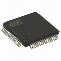
AT90CAN64-16AUR Atmel, AT90CAN64-16AUR Datasheet - Page 351

AT90CAN64-16AUR
Manufacturer Part Number
AT90CAN64-16AUR
Description
MCU AVR 64K FLASH 16MHZ 64TQFP
Manufacturer
Atmel
Series
AVR® 90CANr
Datasheet
1.AT90CAN32-16AUR.pdf
(428 pages)
Specifications of AT90CAN64-16AUR
Core Processor
AVR
Core Size
8-Bit
Speed
16MHz
Connectivity
CAN, EBI/EMI, I²C, SPI, UART/USART
Peripherals
Brown-out Detect/Reset, POR, PWM, WDT
Number Of I /o
53
Program Memory Size
64KB (64K x 8)
Program Memory Type
FLASH
Eeprom Size
2K x 8
Ram Size
4K x 8
Voltage - Supply (vcc/vdd)
2.7 V ~ 5.5 V
Data Converters
A/D 8x10b
Oscillator Type
Internal
Operating Temperature
-40°C ~ 85°C
Package / Case
64-TQFP, 64-VQFP
Data Bus Width
8 bit
Data Ram Size
4 KB
Mounting Style
SMD/SMT
Lead Free Status / RoHS Status
Lead free / RoHS Compliant
Available stocks
Company
Part Number
Manufacturer
Quantity
Price
- Current page: 351 of 428
- Download datasheet (6Mb)
Table 25-15. Serial Programming Instruction Set
7679H–CAN–08/08
Instruction
Programming
Enable
Chip Erase
Read
Program Memory
Load
Program Memory
Page
Write
Program Memory
Page
Read
EEPROM Memory
Write
EEPROM Memory
Set
a = address high bits, b = address low bits, H = 0 - Low byte, 1 - High Byte, o = data out, i = data in, x = don’t care
1010 1100 0101 0011 xxxx xxxx xxxx xxxx Enable Serial Programming after RESET goes low.
1010 1100 100x xxxx xxxx xxxx xxxx xxxx Chip Erase EEPROM and Flash.
0010 H000 aaaa aaaa bbbb bbbb oooo oooo
0100 H000 000x xxxx xbbb bbbb iiii iiii
0100 1100 aaaa aaaa bxxx xxxx xxxx xxxx Write Program Memory Page at address a:b.
1010 0000 000x aaaa bbbb bbbb oooo oooo Read data o from EEPROM memory at address a:b.
1100 0000 000x aaaa bbbb bbbb iiii iiii Write data i to EEPROM memory at address a:b.
Byte 1
are meant to contain 0xFF, can be skipped. This does not apply if the EEPROM is re-pro-
grammed without chip erasing the device. In this case, data polling cannot be used for the value
0xFF, and the user will have to wait at least t
Table 25-14
Table 25-14. Minimum Wait Delay Before Writing the Next Flash or EEPROM Location
Figure 25-8. Serial Programming Waveforms
Symbol
t
t
t
t
WD_FUSE
WD_FLASH
WD_EEPROM
WD_ERASE
SERIAL DA TA OUTPUT
SERIAL CLOCK INPUT
Byte 2
Instruction Format
SERIAL DA TA INPUT
for t
(2)
WD_EEPROM
(MISO-PDO)
(MOSI-PDI)
Sample
(SCK)
Byte 3
value.
(1)
MSB
MSB
Byte4
WD_EEPROM
Operation
Read H (high or low) data o from Program memory at
word address a:b.
Write H (high or low) data i to Program Memory page
at word address b. Data low byte must be loaded
before Data high byte is applied within the same
address.
Minimum Wait Delay
(1)
before programming the next byte. See
AT90CAN32/64/128
4.5 ms
4.5 ms
9.0 ms
9.0 ms
LSB
LSB
351
Related parts for AT90CAN64-16AUR
Image
Part Number
Description
Manufacturer
Datasheet
Request
R

Part Number:
Description:
Manufacturer:
Atmel Corporation
Datasheet:

Part Number:
Description:
Manufacturer:
Atmel Corporation
Datasheet:

Part Number:
Description:
IC MCU AVR 64K FLASH 64-TQFP
Manufacturer:
Atmel
Datasheet:

Part Number:
Description:
IC MCU AVR 64K FLASH 64-QFN
Manufacturer:
Atmel
Datasheet:

Part Number:
Description:
At90can128 8-bit Avr Microcontroller With 32k Bytes Of Isp Flash And Can Controller
Manufacturer:
ATMEL Corporation
Datasheet:

Part Number:
Description:
8-bit Microcontrollers - MCU 64 KB FLASH - 16MHz
Manufacturer:
Atmel

Part Number:
Description:
8-bit Microcontrollers - MCU Microcontroller
Manufacturer:
Atmel

Part Number:
Description:
DEV KIT FOR AVR/AVR32
Manufacturer:
Atmel
Datasheet:


