AT90CAN64-16AUR Atmel, AT90CAN64-16AUR Datasheet - Page 77
AT90CAN64-16AUR
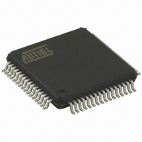
Manufacturer Part Number
AT90CAN64-16AUR
Description
MCU AVR 64K FLASH 16MHZ 64TQFP
Manufacturer
Atmel
Series
AVR® 90CANr
Datasheet
1.AT90CAN32-16AUR.pdf
(428 pages)
Specifications of AT90CAN64-16AUR
Core Processor
AVR
Core Size
8-Bit
Speed
16MHz
Connectivity
CAN, EBI/EMI, I²C, SPI, UART/USART
Peripherals
Brown-out Detect/Reset, POR, PWM, WDT
Number Of I /o
53
Program Memory Size
64KB (64K x 8)
Program Memory Type
FLASH
Eeprom Size
2K x 8
Ram Size
4K x 8
Voltage - Supply (vcc/vdd)
2.7 V ~ 5.5 V
Data Converters
A/D 8x10b
Oscillator Type
Internal
Operating Temperature
-40°C ~ 85°C
Package / Case
64-TQFP, 64-VQFP
Data Bus Width
8 bit
Data Ram Size
4 KB
Mounting Style
SMD/SMT
Lead Free Status / RoHS Status
Lead free / RoHS Compliant
Available stocks
Company
Part Number
Manufacturer
Quantity
Price


7679H–CAN–08/08
MOSI, SPI Master Data output, Slave Data input for SPI channel. When the SPI is enabled as a
slave, this pin is configured as an input regardless of the setting of DDB2. When the SPI is
enabled as a master, the data direction of this pin is controlled by DDB2. When the pin is forced
to be an input, the pull-up can still be controlled by the PORTB2 bit.
• SCK – Port B, Bit 1
SCK, Master Clock output, Slave Clock input pin for SPI channel. When the SPI is enabled as a
slave, this pin is configured as an input regardless of the setting of DDB1. When the SPI is
enabled as a master, the data direction of this pin is controlled by DDB1. When the pin is forced
to be an input, the pull-up can still be controlled by the PORTB1 bit.
• SS – Port B, Bit 0
SS, Slave Port Select input. When the SPI is enabled as a slave, this pin is configured as an
input regardless of the setting of DDB0. As a slave, the SPI is activated when this pin is driven
low. When the SPI is enabled as a master, the data direction of this pin is controlled by DDB0.
When the pin is forced to be an input, the pull-up can still be controlled by the PORTB0 bit.
Table 9-7
in
nal, while MOSI is divided into SPI MSTR OUTPUT and SPI SLAVE INPUT.
Table 9-7
in
Table 9-7.
Note:
Signal Name
PUOE
PUOV
DDOE
DDOV
PVOE
PVOV
PTOE
DIEOE
DIEOV
DI
AIO
Figure 9-5 on page
Figure 9-5 on page
1. See
and
and
Table 9-8
Overriding Signals for Alternate Functions in PB7..PB4
Table 9-8
“Output Compare Modulator - OCM” on page 165
PB7/OC0A/OC1C
0
0
0
0
OC0A/OC1C
ENABLE
OC0A/OC1C
0
0
0
–
–
72.
72. SPI MSTR INPUT and SPI SLAVE OUTPUT constitute the MISO sig-
relates the alternate functions of Port B to the overriding signals shown
relate the alternate functions of Port B to the overriding signals shown
(1)
(1)
PB6/OC1B
0
0
0
0
OC1B ENABLE
OC1B
0
0
0
–
–
AT90CAN32/64/128
PB5/OC1A
0
0
0
0
OC1A ENABLE
OC1A
0
0
0
–
–
for details.
PB4/OC2A
0
0
0
0
OC2A ENABLE
OC2A
0
0
0
–
–
77
Related parts for AT90CAN64-16AUR
Image
Part Number
Description
Manufacturer
Datasheet
Request
R

Part Number:
Description:
Manufacturer:
Atmel Corporation
Datasheet:
Part Number:
Description:
Manufacturer:
Atmel Corporation
Datasheet:

Part Number:
Description:
IC MCU AVR 64K FLASH 64-TQFP
Manufacturer:
Atmel
Datasheet:

Part Number:
Description:
IC MCU AVR 64K FLASH 64-QFN
Manufacturer:
Atmel
Datasheet:

Part Number:
Description:
At90can128 8-bit Avr Microcontroller With 32k Bytes Of Isp Flash And Can Controller
Manufacturer:
ATMEL Corporation
Datasheet:

Part Number:
Description:
8-bit Microcontrollers - MCU 64 KB FLASH - 16MHz
Manufacturer:
Atmel
Part Number:
Description:
8-bit Microcontrollers - MCU Microcontroller
Manufacturer:
Atmel

Part Number:
Description:
DEV KIT FOR AVR/AVR32
Manufacturer:
Atmel
Datasheet: