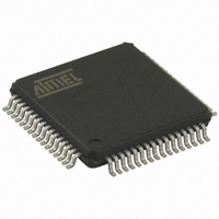
AT32UC3B0512-A2UT Atmel, AT32UC3B0512-A2UT Datasheet - Page 208

AT32UC3B0512-A2UT
Manufacturer Part Number
AT32UC3B0512-A2UT
Description
IC MCU AVR32 512K FLASH 64TQFP
Manufacturer
Atmel
Series
AVR®32 UC3r
Specifications of AT32UC3B0512-A2UT
Core Processor
AVR
Core Size
32-Bit
Speed
60MHz
Connectivity
I²C, IrDA, SPI, SSC, UART/USART, USB
Peripherals
Brown-out Detect/Reset, DMA, POR, PWM, WDT
Number Of I /o
44
Program Memory Size
512KB (512K x 8)
Program Memory Type
FLASH
Ram Size
96K x 8
Voltage - Supply (vcc/vdd)
1.65 V ~ 1.95 V
Data Converters
A/D 8x10b
Oscillator Type
Internal
Operating Temperature
-40°C ~ 85°C
Package / Case
64-TQFP, 64-VQFP
Controller Family/series
AT32UC3B
No. Of I/o's
44
Ram Memory Size
96KB
Cpu Speed
60MHz
No. Of Timers
1
Rohs Compliant
Yes
Lead Free Status / RoHS Status
Lead free / RoHS Compliant
Eeprom Size
-
Available stocks
Company
Part Number
Manufacturer
Quantity
Price
Company:
Part Number:
AT32UC3B0512-A2UT
Manufacturer:
MURATA
Quantity:
11 450
Part Number:
AT32UC3B0512-A2UT
Manufacturer:
ATMEL/爱特梅尔
Quantity:
20 000
- Current page: 208 of 692
- Download datasheet (11Mb)
18.8.2
Name:
Access Type:
Offset:
Reset Value:
• DLYBCS: Delay Between Chip Selects
• PCS: Peripheral Chip Select
• LLB: Local Loopback Enable
• MODFDIS: Mode Fault Detection
• PCSDEC: Chip Select Decode
32059K–03/2011
LLB
31
23
15
–
–
7
This field defines the delay from NPCS inactive to the activation of another NPCS. The DLYBCS time guarantees non-
overlapping chip selects and solves bus contentions in case of peripherals having long data float times.
If DLYBCS is less than or equal to six, six CLK_SPI periods will be inserted by default.
Otherwise, the following equation determines the delay:
This field is only used if Fixed Peripheral Select is active (PS = 0).
If PCSDEC = 0:
PCS = xxx0NPCS[3:0] = 1110
PCS = xx01NPCS[3:0] = 1101
PCS = x011NPCS[3:0] = 1011
PCS = 0111NPCS[3:0] = 0111
PCS = 1111forbidden (no peripheral is selected)
(x = don’t care)
If PCSDEC = 1:
NPCS[3:0] output signals = PCS.
0: Local loopback path disabled.
1: Local loopback path enabled (
LLB controls the local loopback on the data serializer for testing in Master Mode only. (MISO is internally connected on MOSI.)
0: Mode fault detection is enabled.
1: Mode fault detection is disabled.
0: The chip selects are directly connected to a peripheral device.
1: The four chip select lines are connected to a 4- to 16-bit decoder.
When PCSDEC equals one, up to 15 Chip Select signals can be generated with the four lines using an external 4- to 16-bit
decoder. The Chip Select Registers define the characteristics of the 15 chip selects according to the following rules:
CSR0 defines peripheral chip select signals 0 to 3.
CSR1 defines peripheral chip select signals 4 to 7.
CSR2 defines peripheral chip select signals 8 to 11.
Delay Between Chip Selects
Mode Register
30
22
14
MR
Read/Write
0x04
0x00000000
–
–
6
-
29
21
13
–
–
5
-
=
DLYBCS
---------------------- -
CLKSPI
MODFDIS
28
20
12
–
–
4
DLYBCS
27
19
11
–
3
–
PCSDEC
26
18
10
–
2
PCS
PS
25
17
–
9
1
AT32UC3B
MSTR
24
16
–
8
0
208
Related parts for AT32UC3B0512-A2UT
Image
Part Number
Description
Manufacturer
Datasheet
Request
R

Part Number:
Description:
DEV KIT FOR AVR/AVR32
Manufacturer:
Atmel
Datasheet:

Part Number:
Description:
INTERVAL AND WIPE/WASH WIPER CONTROL IC WITH DELAY
Manufacturer:
ATMEL Corporation
Datasheet:

Part Number:
Description:
Low-Voltage Voice-Switched IC for Hands-Free Operation
Manufacturer:
ATMEL Corporation
Datasheet:

Part Number:
Description:
MONOLITHIC INTEGRATED FEATUREPHONE CIRCUIT
Manufacturer:
ATMEL Corporation
Datasheet:

Part Number:
Description:
AM-FM Receiver IC U4255BM-M
Manufacturer:
ATMEL Corporation
Datasheet:

Part Number:
Description:
Monolithic Integrated Feature Phone Circuit
Manufacturer:
ATMEL Corporation
Datasheet:

Part Number:
Description:
Multistandard Video-IF and Quasi Parallel Sound Processing
Manufacturer:
ATMEL Corporation
Datasheet:

Part Number:
Description:
High-performance EE PLD
Manufacturer:
ATMEL Corporation
Datasheet:

Part Number:
Description:
8-bit Flash Microcontroller
Manufacturer:
ATMEL Corporation
Datasheet:

Part Number:
Description:
2-Wire Serial EEPROM
Manufacturer:
ATMEL Corporation
Datasheet:


