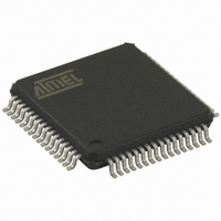
AT32UC3B0512-A2UT Atmel, AT32UC3B0512-A2UT Datasheet - Page 222

AT32UC3B0512-A2UT
Manufacturer Part Number
AT32UC3B0512-A2UT
Description
IC MCU AVR32 512K FLASH 64TQFP
Manufacturer
Atmel
Series
AVR®32 UC3r
Specifications of AT32UC3B0512-A2UT
Core Processor
AVR
Core Size
32-Bit
Speed
60MHz
Connectivity
I²C, IrDA, SPI, SSC, UART/USART, USB
Peripherals
Brown-out Detect/Reset, DMA, POR, PWM, WDT
Number Of I /o
44
Program Memory Size
512KB (512K x 8)
Program Memory Type
FLASH
Ram Size
96K x 8
Voltage - Supply (vcc/vdd)
1.65 V ~ 1.95 V
Data Converters
A/D 8x10b
Oscillator Type
Internal
Operating Temperature
-40°C ~ 85°C
Package / Case
64-TQFP, 64-VQFP
Controller Family/series
AT32UC3B
No. Of I/o's
44
Ram Memory Size
96KB
Cpu Speed
60MHz
No. Of Timers
1
Rohs Compliant
Yes
Lead Free Status / RoHS Status
Lead free / RoHS Compliant
Eeprom Size
-
Available stocks
Company
Part Number
Manufacturer
Quantity
Price
Company:
Part Number:
AT32UC3B0512-A2UT
Manufacturer:
MURATA
Quantity:
11 450
Part Number:
AT32UC3B0512-A2UT
Manufacturer:
ATMEL/爱特梅尔
Quantity:
20 000
- Current page: 222 of 692
- Download datasheet (11Mb)
19.10 Master Mode
19.10.1
19.10.2
Figure 19-5. Master Mode Typical Application Block Diagram
19.10.3
19.10.4
19.10.5
32059K–03/2011
Definition
Application Block Diagram
Programming Master Mode
Master Mode Clock Timing
Master Transmitter Mode
Rp: Pull up value as given by the I²C Standard
Host with
Interface
TWI
The Master is the device which starts a transfer, generates a clock and stops it.
The following registers have to be programmed before entering Master mode:
The TWI module monitors the state of the TWCK line as required by the I²C specification. The
counter that determines the TWCK T
is detected by the module on TWCK, not when the module begins releasing or driving the TWCK
line. Thus, the CWGR.CHDIV and CLDIV fields do not alone determine the overall TWCK
period; they merely determine the T
(T
tion and synchronization delay of TWCK from the pin back into the TWI module. The TWI
module does not attempt to compensate for these delays, so the overall TWI clock period is
given by T
After the master initiates a Start condition when writing into the Transmit Holding Register, THR,
it sends a 7-bit slave address, configured in the Master Mode register (DADR in MMR), to notify
the slave device. The bit following the slave address indicates the transfer direction, 0 in this
case (MREAD = 0 in MMR).
TWD
TWCK
1. DADR (+ IADRSZ + IADR if a 10 bit device is addressed): The device address is used
2. CKDIV + CHDIV + CLDIV: Determines clock waveform T
3. SVDIS: Disable the slave mode.
4. MSEN: Enable the master mode.
rise
Serial EEPROM
and T
to access slave devices in read or write mode.
Atmel TWI
Slave 1
high
fall
) are determined by the external circuitry on the TWCK pin as well as the propaga-
+T
fall
+T
low
+T
I²C RTC
Slave 2
rise
.
high
high
Controller
I²C LCD
Slave 3
or T
and T
low
low
duration is started whenever a high or low level
components, whereas the rise and fall times
I²C Temp.
Slave 4
Sensor
Rp
high
and T
Rp
low
.
AT32UC3B
VDD
222
Related parts for AT32UC3B0512-A2UT
Image
Part Number
Description
Manufacturer
Datasheet
Request
R

Part Number:
Description:
DEV KIT FOR AVR/AVR32
Manufacturer:
Atmel
Datasheet:

Part Number:
Description:
INTERVAL AND WIPE/WASH WIPER CONTROL IC WITH DELAY
Manufacturer:
ATMEL Corporation
Datasheet:

Part Number:
Description:
Low-Voltage Voice-Switched IC for Hands-Free Operation
Manufacturer:
ATMEL Corporation
Datasheet:

Part Number:
Description:
MONOLITHIC INTEGRATED FEATUREPHONE CIRCUIT
Manufacturer:
ATMEL Corporation
Datasheet:

Part Number:
Description:
AM-FM Receiver IC U4255BM-M
Manufacturer:
ATMEL Corporation
Datasheet:

Part Number:
Description:
Monolithic Integrated Feature Phone Circuit
Manufacturer:
ATMEL Corporation
Datasheet:

Part Number:
Description:
Multistandard Video-IF and Quasi Parallel Sound Processing
Manufacturer:
ATMEL Corporation
Datasheet:

Part Number:
Description:
High-performance EE PLD
Manufacturer:
ATMEL Corporation
Datasheet:

Part Number:
Description:
8-bit Flash Microcontroller
Manufacturer:
ATMEL Corporation
Datasheet:

Part Number:
Description:
2-Wire Serial EEPROM
Manufacturer:
ATMEL Corporation
Datasheet:


