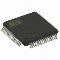
AT32UC3B0512-A2UT Atmel, AT32UC3B0512-A2UT Datasheet - Page 680

AT32UC3B0512-A2UT
Manufacturer Part Number
AT32UC3B0512-A2UT
Description
IC MCU AVR32 512K FLASH 64TQFP
Manufacturer
Atmel
Series
AVR®32 UC3r
Specifications of AT32UC3B0512-A2UT
Core Processor
AVR
Core Size
32-Bit
Speed
60MHz
Connectivity
I²C, IrDA, SPI, SSC, UART/USART, USB
Peripherals
Brown-out Detect/Reset, DMA, POR, PWM, WDT
Number Of I /o
44
Program Memory Size
512KB (512K x 8)
Program Memory Type
FLASH
Ram Size
96K x 8
Voltage - Supply (vcc/vdd)
1.65 V ~ 1.95 V
Data Converters
A/D 8x10b
Oscillator Type
Internal
Operating Temperature
-40°C ~ 85°C
Package / Case
64-TQFP, 64-VQFP
Controller Family/series
AT32UC3B
No. Of I/o's
44
Ram Memory Size
96KB
Cpu Speed
60MHz
No. Of Timers
1
Rohs Compliant
Yes
Lead Free Status / RoHS Status
Lead free / RoHS Compliant
Eeprom Size
-
Available stocks
Company
Part Number
Manufacturer
Quantity
Price
Company:
Part Number:
AT32UC3B0512-A2UT
Manufacturer:
MURATA
Quantity:
11 450
Part Number:
AT32UC3B0512-A2UT
Manufacturer:
ATMEL/爱特梅尔
Quantity:
20 000
- Current page: 680 of 692
- Download datasheet (11Mb)
32059K–03/2011
- RTC
- OCD
3. PAGEN Semantic Field for Program GP Fuse Byte is WriteData[7:0], ByteAddress[1:0]
4. Reading from on-chip flash may fail after a flash fuse write operation (FLASHC LP,
1. Writes to control (CTRL), top (TOP) and value (VAL) in the RTC are discarded if the
2. The RTC CLKEN bit (bit number 16) of CTRL register is not available
1. Stalled memory access instruction writeback fails if followed by a HW breakpoint
on revision B instead of WriteData[7:0], ByteAddress[2:0]
PAGEN Semantic Field for Program GP Fuse Byte is WriteData[7:0], ByteAddress[1:0] on
revision B instead of WriteData[7:0], ByteAddress[2:0].
Fix/Workaround
None.
UP, WGPB, EGPB, SSB, PGPFB, EAGPF commands).
After a flash fuse write operation (FLASHC LP, UP, WGPB, EGPB, SSB, PGPFB, EAGPF
commands), the following flash read access may return corrupted data. This erratum does
not affect write operations to regular flash memory.
Fix/Workaround
The flash fuse write operation (FLASHC LP, UP, WGPB, EGPB, SSB, PGPFB, EAGPF
commands) must be issued from internal RAM. After the write operation, perform a dummy
flash page write operation (FLASHC WP). Content and location of this page is not important
and filling the write buffer with all one (FFh) will leave the current flash content unchanged. It
is then safe to read and fetch code from the flash.
RTC peripheral bus clock (PBA) is divided by a factor of four or more relative to the
HSB clock
Writes to control (CTRL), top (TOP) and value (VAL) in the RTC are discarded if the RTC
peripheral bus clock (PBA) is divided by a factor of four or more relative to the HSB clock.
Fix/Workaround
Do not write to the RTC registers using the peripheral bus clock (PBA) divided by a factor of
four or more relative to the HSB clock.
The RTC CLKEN bit (bit number 16) of CTRL register is not available.
Fix/Workaround
Do not use the CLKEN bit of the RTC on Rev B.
Consider the following assembly code sequence:
A
B
If a hardware breakpoint is placed on instruction B, and instruction A is a memory access
instruction, register file updates from instruction A can be discarded.
Fix/Workaround
Do not place hardware breakpoints, use software breakpoints instead. Alternatively, place a
hardware breakpoint on the instruction before the memory access instruction and then sin-
gle step over the memory access instruction.
AT32UC3B
680
Related parts for AT32UC3B0512-A2UT
Image
Part Number
Description
Manufacturer
Datasheet
Request
R

Part Number:
Description:
DEV KIT FOR AVR/AVR32
Manufacturer:
Atmel
Datasheet:

Part Number:
Description:
INTERVAL AND WIPE/WASH WIPER CONTROL IC WITH DELAY
Manufacturer:
ATMEL Corporation
Datasheet:

Part Number:
Description:
Low-Voltage Voice-Switched IC for Hands-Free Operation
Manufacturer:
ATMEL Corporation
Datasheet:

Part Number:
Description:
MONOLITHIC INTEGRATED FEATUREPHONE CIRCUIT
Manufacturer:
ATMEL Corporation
Datasheet:

Part Number:
Description:
AM-FM Receiver IC U4255BM-M
Manufacturer:
ATMEL Corporation
Datasheet:

Part Number:
Description:
Monolithic Integrated Feature Phone Circuit
Manufacturer:
ATMEL Corporation
Datasheet:

Part Number:
Description:
Multistandard Video-IF and Quasi Parallel Sound Processing
Manufacturer:
ATMEL Corporation
Datasheet:

Part Number:
Description:
High-performance EE PLD
Manufacturer:
ATMEL Corporation
Datasheet:

Part Number:
Description:
8-bit Flash Microcontroller
Manufacturer:
ATMEL Corporation
Datasheet:

Part Number:
Description:
2-Wire Serial EEPROM
Manufacturer:
ATMEL Corporation
Datasheet:


