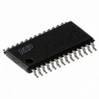
P89LPC9381FDH,512 NXP Semiconductors, P89LPC9381FDH,512 Datasheet - Page 39

P89LPC9381FDH,512
Manufacturer Part Number
P89LPC9381FDH,512
Description
IC 80C51 MCU FLASH 4K 28-TSSOP
Manufacturer
NXP Semiconductors
Series
LPC900r
Datasheet
1.P89LPC9381FA112.pdf
(60 pages)
Specifications of P89LPC9381FDH,512
Core Processor
8051
Core Size
8-Bit
Speed
18MHz
Connectivity
I²C, SPI, UART/USART
Peripherals
Brown-out Detect/Reset, LED, POR, PWM, WDT
Number Of I /o
26
Program Memory Size
4KB (4K x 8)
Program Memory Type
FLASH
Ram Size
256 x 8
Voltage - Supply (vcc/vdd)
2.4 V ~ 3.6 V
Data Converters
A/D 8x10b
Oscillator Type
Internal
Operating Temperature
-40°C ~ 85°C
Package / Case
28-TSSOP
Processor Series
P89LPC9x
Core
80C51
Data Bus Width
8 bit
Data Ram Size
256 B
Interface Type
I2C, SPI, UART
Maximum Clock Frequency
18 MHz
Number Of Programmable I/os
26
Number Of Timers
2
Operating Supply Voltage
2.4 V to 3.6 V
Maximum Operating Temperature
+ 85 C
Mounting Style
SMD/SMT
3rd Party Development Tools
PK51, CA51, A51, ULINK2
Minimum Operating Temperature
- 40 C
On-chip Adc
10 bit, 8 Channel
For Use With
622-1014 - BOARD FOR LPC9XX TSSOP622-1011 - BOARD FOR LPC938 TSSOP622-1008 - BOARD FOR LPC9103 10-HVSON622-1006 - SOCKET ADAPTER BOARDMCB900K - BOARD PROTOTYPE NXP 89LPC9EPM900K - EMULATOR/PROGRAMMER NXP P89LPC9568-1759 - EMULATOR DEBUGGER/PROGRMMR LPC9X568-1758 - BOARD EVAL FOR LPC93X MCU FAMILY
Lead Free Status / RoHS Status
Lead free / RoHS Compliant
Eeprom Size
-
Lead Free Status / Rohs Status
Details
Other names
935280615512
P89LPC9381FDH
P89LPC9381FDH
P89LPC9381FDH
P89LPC9381FDH
Available stocks
Company
Part Number
Manufacturer
Quantity
Price
Company:
Part Number:
P89LPC9381FDH,512
Manufacturer:
LT
Quantity:
2 340
Philips Semiconductors
8. ADC
P89LPC9381_1
Product data sheet
7.26.10 Hardware activation of the bootloader
7.26.9 Power-on reset code execution
7.27 User configuration bytes
7.28 User sector security bytes
8.1 General description
The P89LPC9381 contains two special flash elements: the Boot Vector and the Boot
Status Bit. Following reset, the P89LPC9381 examines the contents of the Boot Status
Bit. If the Boot Status Bit is set to zero, power-up execution starts at location 0000H, which
is the normal start address of the user’s application code. When the Boot Status Bit is set
to a value other than zero, the contents of the Boot Vector is used as the high byte of the
execution address and the low byte is set to 00H.
Table 8
bootloader is pre-programmed into the address space indicated and uses the indicated
boot loader entry point to perform ISP functions. This code can be erased by the user.
Users who wish to use this loader should take precautions to avoid erasing the
1 kB sector that contains this boot loader. Instead, the page erase function can be
used to erase the first eight 64 B pages located in this sector. A custom bootloader
can be written with the Boot Vector set to the custom boot loader, if desired.
Table 8.
The bootloader can also be executed by forcing the device into ISP mode during a
power-on sequence (see the P89LPC9381 User’s Manual for specific information). This
has the same effect as having a non-zero status byte. This allows an application to be built
that will normally execute user code but can be manually forced into ISP operation. If the
factory default setting for the Boot Vector (0FH) is changed, it will no longer point to the
factory pre-programmed ISP bootloader code. After programming the flash, the status
byte should be programmed to zero in order to allow execution of the user’s application
code beginning at address 0000H.
Some user-configurable features of the P89LPC9381 must be defined at power-up and
therefore cannot be set by the program after start of execution. These features are
configured through the use of the flash byte UCFG1. Please see the P89LPC9381 User’s
Manual for additional details.
There are four User Sector Security Bytes on the P89LPC9381. Each byte corresponds to
one sector. Please see the P89LPC9381 User’s Manual for additional details.
The P89LPC9381 has a 10-bit, 8-channel multiplexed successive approximation
analog-to-digital converter module. A block diagram of the ADC is shown in
The ADC consists of an 8-input multiplexer which feeds a sample-and-hold circuit
Device
P89LPC9381
shows the factory default Boot Vector setting for this device. A factory-provided
Default Boot Vector values and ISP entry points
Default
boot vector
0FH
Rev. 01 — 8 September 2006
Default
bootloader
entry point
0F00H
8-bit microcontroller with 10-bit ADC
Default bootloader
code range
0E00H to 0FFFH
© Koninklijke Philips Electronics N.V. 2006. All rights reserved.
P89LPC9381
1 kB sector
range
0C00H to 0FFFH
Figure
15.
39 of 60


