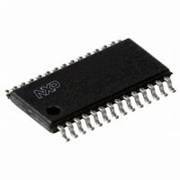
P89LPC9381FDH,512 NXP Semiconductors, P89LPC9381FDH,512 Datasheet - Page 6

P89LPC9381FDH,512
Manufacturer Part Number
P89LPC9381FDH,512
Description
IC 80C51 MCU FLASH 4K 28-TSSOP
Manufacturer
NXP Semiconductors
Series
LPC900r
Datasheet
1.P89LPC9381FA112.pdf
(60 pages)
Specifications of P89LPC9381FDH,512
Core Processor
8051
Core Size
8-Bit
Speed
18MHz
Connectivity
I²C, SPI, UART/USART
Peripherals
Brown-out Detect/Reset, LED, POR, PWM, WDT
Number Of I /o
26
Program Memory Size
4KB (4K x 8)
Program Memory Type
FLASH
Ram Size
256 x 8
Voltage - Supply (vcc/vdd)
2.4 V ~ 3.6 V
Data Converters
A/D 8x10b
Oscillator Type
Internal
Operating Temperature
-40°C ~ 85°C
Package / Case
28-TSSOP
Processor Series
P89LPC9x
Core
80C51
Data Bus Width
8 bit
Data Ram Size
256 B
Interface Type
I2C, SPI, UART
Maximum Clock Frequency
18 MHz
Number Of Programmable I/os
26
Number Of Timers
2
Operating Supply Voltage
2.4 V to 3.6 V
Maximum Operating Temperature
+ 85 C
Mounting Style
SMD/SMT
3rd Party Development Tools
PK51, CA51, A51, ULINK2
Minimum Operating Temperature
- 40 C
On-chip Adc
10 bit, 8 Channel
For Use With
622-1014 - BOARD FOR LPC9XX TSSOP622-1011 - BOARD FOR LPC938 TSSOP622-1008 - BOARD FOR LPC9103 10-HVSON622-1006 - SOCKET ADAPTER BOARDMCB900K - BOARD PROTOTYPE NXP 89LPC9EPM900K - EMULATOR/PROGRAMMER NXP P89LPC9568-1759 - EMULATOR DEBUGGER/PROGRMMR LPC9X568-1758 - BOARD EVAL FOR LPC93X MCU FAMILY
Lead Free Status / RoHS Status
Lead free / RoHS Compliant
Eeprom Size
-
Lead Free Status / Rohs Status
Details
Other names
935280615512
P89LPC9381FDH
P89LPC9381FDH
P89LPC9381FDH
P89LPC9381FDH
Available stocks
Company
Part Number
Manufacturer
Quantity
Price
Company:
Part Number:
P89LPC9381FDH,512
Manufacturer:
LT
Quantity:
2 340
Philips Semiconductors
6. Pinning information
Table 3.
P89LPC9381_1
Product data sheet
Symbol
P0[7:0]
P0[0]/CMP2/
KBI0/AD05
P0[1]/CIN2B/
KBI1/AD00
Pin description
6.1 Pinning
6.2 Pin description
Pin
3
26
Fig 3. Pin configuration
Type Description
I/O
I/O
O
I
I
I/O
I
I
I
P0[0]/CMP2/KBI0/AD05
Port 0: Port 0 is an 8-bit I/O port with a user-configurable output type. During reset
Port 0 latches are configured in the input only mode with the internal pull-up
disabled. The operation of Port 0 pins as inputs and outputs depends upon the
port configuration selected. Each port pin is configured independently. Refer to
Section 7.13.1 “Port configurations”
details.
The Keypad Interrupt feature operates with Port 0 pins.
All pins have Schmitt triggered inputs.
Port 0 also provides various special functions as described below:
P0[0] — Port 0 bit 0.
CMP2 — Comparator 2 output.
KBI0 — Keyboard input 0.
AD05 — ADC0 channel 5 analog input.
P0[1] — Port 0 bit 1.
CIN2B — Comparator 2 positive input B.
KBI1 — Keyboard input 1.
AD00 — ADC0 channel 0 analog input.
P3[0]/XTAL2/CLKOUT
P1[3]/INT0/SDA
Rev. 01 — 8 September 2006
P1[2]/T0/SCL
P3[1]/XTAL1
P2[2]/MOSI
P2[3]/MISO
P2[0]/AD07
P2[1]/AD06
P1[7]/AD04
P1[4]/INT1
P1[5]/RST
P1[6]
V
SS
10
11
12
13
14
1
2
3
4
5
6
7
8
9
P89LPC9381
and
002aac462
8-bit microcontroller with 10-bit ADC
Table 10 “Static characteristics”
28
27
26
25
24
23
22
21
20
19
18
17
16
15
P2[7]
P2[6]
P0[1]/CIN2B/KBI1/AD00
P0[2]/CIN2A/KBI2/AD01
P0[3]/CIN1B/KBI3/AD02
P0[4]/CIN1A/KBI4/AD03
P0[5]/CMPREF/KBI5
V
P0[6]/CMP1/KBI6
P0[7]/T1/KBI7
P1[0]/TXD
P1[1]/RXD
P2[5]/SPICLK
P2[4]/SS
© Koninklijke Philips Electronics N.V. 2006. All rights reserved.
DD
P89LPC9381
for
6 of 60


