P89LPC9381FDH,512 NXP Semiconductors, P89LPC9381FDH,512 Datasheet - Page 9
P89LPC9381FDH,512
Manufacturer Part Number
P89LPC9381FDH,512
Description
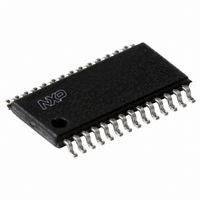
IC 80C51 MCU FLASH 4K 28-TSSOP
Manufacturer
NXP Semiconductors
Series
LPC900r
Datasheet
1.P89LPC9381FA112.pdf
(60 pages)
Specifications of P89LPC9381FDH,512
Core Processor
8051
Core Size
8-Bit
Speed
18MHz
Connectivity
I²C, SPI, UART/USART
Peripherals
Brown-out Detect/Reset, LED, POR, PWM, WDT
Number Of I /o
26
Program Memory Size
4KB (4K x 8)
Program Memory Type
FLASH
Ram Size
256 x 8
Voltage - Supply (vcc/vdd)
2.4 V ~ 3.6 V
Data Converters
A/D 8x10b
Oscillator Type
Internal
Operating Temperature
-40°C ~ 85°C
Package / Case
28-TSSOP
Processor Series
P89LPC9x
Core
80C51
Data Bus Width
8 bit
Data Ram Size
256 B
Interface Type
I2C, SPI, UART
Maximum Clock Frequency
18 MHz
Number Of Programmable I/os
26
Number Of Timers
2
Operating Supply Voltage
2.4 V to 3.6 V
Maximum Operating Temperature
+ 85 C
Mounting Style
SMD/SMT
3rd Party Development Tools
PK51, CA51, A51, ULINK2
Minimum Operating Temperature
- 40 C
On-chip Adc
10 bit, 8 Channel
For Use With
622-1014 - BOARD FOR LPC9XX TSSOP622-1011 - BOARD FOR LPC938 TSSOP622-1008 - BOARD FOR LPC9103 10-HVSON622-1006 - SOCKET ADAPTER BOARDMCB900K - BOARD PROTOTYPE NXP 89LPC9EPM900K - EMULATOR/PROGRAMMER NXP P89LPC9568-1759 - EMULATOR DEBUGGER/PROGRMMR LPC9X568-1758 - BOARD EVAL FOR LPC93X MCU FAMILY
Lead Free Status / RoHS Status
Lead free / RoHS Compliant
Eeprom Size
-
Lead Free Status / Rohs Status
Details
Other names
935280615512
P89LPC9381FDH
P89LPC9381FDH
P89LPC9381FDH
P89LPC9381FDH
Available stocks
Company
Part Number
Manufacturer
Quantity
Price
Company:

Part Number:
P89LPC9381FDH,512
Manufacturer:
LT
Quantity:
2 340


Philips Semiconductors
Table 3.
[1]
P89LPC9381_1
Product data sheet
Symbol
P3[1:0]
P3[0]/XTAL2/
CLKOUT
P3[1]/XTAL1
V
V
SS
DD
Input/output for P1[0] to P1[4], P1[6], P1[7]. Input for P1[5].
Pin description
Pin
9
8
7
21
…continued
Type Description
I/O
I/O
O
O
I/O
I
I
I
Port 3: Port 3 is a 2-bit I/O port with a user-configurable output type. During reset
Port 3 latches are configured in the input only mode with the internal pull-up
disabled. The operation of Port 3 pins as inputs and outputs depends upon the
port configuration selected. Each port pin is configured independently. Refer to
Section 7.13.1 “Port configurations”
details.
All pins have Schmitt triggered inputs.
Port 3 also provides various special functions as described below:
P3[0] — Port 3 bit 0.
XTAL2 — Output from the oscillator amplifier (when a crystal oscillator option is
selected via the flash configuration.
CLKOUT — CPU clock divided by 2 when enabled via SFR bit (ENCLK -TRIM.6).
It can be used if the CPU clock is the internal RC oscillator, watchdog oscillator or
external clock input, except when XTAL1/XTAL2 are used to generate clock source
for the RTC/system timer.
P3[1] — Port 3 bit 1.
XTAL1 — Input to the oscillator circuit and internal clock generator circuits (when
selected via the flash configuration). It can be a port pin if internal RC oscillator or
watchdog oscillator is used as the CPU clock source, and if XTAL1/XTAL2 are not
used to generate the clock for the RTC/system timer.
ground: 0 V reference.
power supply: This is the power supply voltage for normal operation as well as
Idle and Power-down modes.
Rev. 01 — 8 September 2006
and
8-bit microcontroller with 10-bit ADC
Table 10 “Static characteristics”
© Koninklijke Philips Electronics N.V. 2006. All rights reserved.
P89LPC9381
for
9 of 60
Related parts for P89LPC9381FDH,512
Image
Part Number
Description
Manufacturer
Datasheet
Request
R

Part Number:
Description:
The P89LPC9381 is a single-chip microcontroller, available in low-cost packages, basedon a high performance processor architecture that executes instructions in two to fourclocks, six times the rate of standard 80C51 devices
Manufacturer:
NXP Semiconductors
Datasheet:
Part Number:
Description:
The P89LPC938 is a single-chip microcontroller, available in low cost packages, based ona high performance processor architecture that executes instructions in two to four clocks,six times the rate of standard 80C51 devices
Manufacturer:
NXP Semiconductors
Datasheet:
Part Number:
Description:
NXP Semiconductors designed the LPC2420/2460 microcontroller around a 16-bit/32-bitARM7TDMI-S CPU core with real-time debug interfaces that include both JTAG andembedded trace
Manufacturer:
NXP Semiconductors
Datasheet:

Part Number:
Description:
NXP Semiconductors designed the LPC2458 microcontroller around a 16-bit/32-bitARM7TDMI-S CPU core with real-time debug interfaces that include both JTAG andembedded trace
Manufacturer:
NXP Semiconductors
Datasheet:
Part Number:
Description:
NXP Semiconductors designed the LPC2468 microcontroller around a 16-bit/32-bitARM7TDMI-S CPU core with real-time debug interfaces that include both JTAG andembedded trace
Manufacturer:
NXP Semiconductors
Datasheet:
Part Number:
Description:
NXP Semiconductors designed the LPC2470 microcontroller, powered by theARM7TDMI-S core, to be a highly integrated microcontroller for a wide range ofapplications that require advanced communications and high quality graphic displays
Manufacturer:
NXP Semiconductors
Datasheet:
Part Number:
Description:
NXP Semiconductors designed the LPC2478 microcontroller, powered by theARM7TDMI-S core, to be a highly integrated microcontroller for a wide range ofapplications that require advanced communications and high quality graphic displays
Manufacturer:
NXP Semiconductors
Datasheet:
Part Number:
Description:
The Philips Semiconductors XA (eXtended Architecture) family of 16-bit single-chip microcontrollers is powerful enough to easily handle the requirements of high performance embedded applications, yet inexpensive enough to compete in the market for hi
Manufacturer:
NXP Semiconductors
Datasheet:
Part Number:
Description:
The XA-S3 device is a member of Philips Semiconductors? XA(eXtended Architecture) family of high performance 16-bitsingle-chip microcontrollers
Manufacturer:
NXP Semiconductors
Datasheet:

Part Number:
Description:
The NXP BlueStreak LH75401/LH75411 family consists of two low-cost 16/32-bit System-on-Chip (SoC) devices
Manufacturer:
NXP Semiconductors
Datasheet:
Part Number:
Description:
The NXP LPC3130/3131 combine an 180 MHz ARM926EJ-S CPU core, high-speed USB2
Manufacturer:
NXP Semiconductors
Datasheet:
Part Number:
Description:
The NXP LPC3141 combine a 270 MHz ARM926EJ-S CPU core, High-speed USB 2
Manufacturer:
NXP Semiconductors
Part Number:
Description:
The NXP LPC3143 combine a 270 MHz ARM926EJ-S CPU core, High-speed USB 2
Manufacturer:
NXP Semiconductors

Part Number:
Description:
The NXP LPC3152 combines an 180 MHz ARM926EJ-S CPU core, High-speed USB 2
Manufacturer:
NXP Semiconductors