P89LPC9381FDH,512 NXP Semiconductors, P89LPC9381FDH,512 Datasheet - Page 42
P89LPC9381FDH,512
Manufacturer Part Number
P89LPC9381FDH,512
Description
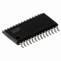
IC 80C51 MCU FLASH 4K 28-TSSOP
Manufacturer
NXP Semiconductors
Series
LPC900r
Datasheet
1.P89LPC9381FA112.pdf
(60 pages)
Specifications of P89LPC9381FDH,512
Core Processor
8051
Core Size
8-Bit
Speed
18MHz
Connectivity
I²C, SPI, UART/USART
Peripherals
Brown-out Detect/Reset, LED, POR, PWM, WDT
Number Of I /o
26
Program Memory Size
4KB (4K x 8)
Program Memory Type
FLASH
Ram Size
256 x 8
Voltage - Supply (vcc/vdd)
2.4 V ~ 3.6 V
Data Converters
A/D 8x10b
Oscillator Type
Internal
Operating Temperature
-40°C ~ 85°C
Package / Case
28-TSSOP
Processor Series
P89LPC9x
Core
80C51
Data Bus Width
8 bit
Data Ram Size
256 B
Interface Type
I2C, SPI, UART
Maximum Clock Frequency
18 MHz
Number Of Programmable I/os
26
Number Of Timers
2
Operating Supply Voltage
2.4 V to 3.6 V
Maximum Operating Temperature
+ 85 C
Mounting Style
SMD/SMT
3rd Party Development Tools
PK51, CA51, A51, ULINK2
Minimum Operating Temperature
- 40 C
On-chip Adc
10 bit, 8 Channel
For Use With
622-1014 - BOARD FOR LPC9XX TSSOP622-1011 - BOARD FOR LPC938 TSSOP622-1008 - BOARD FOR LPC9103 10-HVSON622-1006 - SOCKET ADAPTER BOARDMCB900K - BOARD PROTOTYPE NXP 89LPC9EPM900K - EMULATOR/PROGRAMMER NXP P89LPC9568-1759 - EMULATOR DEBUGGER/PROGRMMR LPC9X568-1758 - BOARD EVAL FOR LPC93X MCU FAMILY
Lead Free Status / RoHS Status
Lead free / RoHS Compliant
Eeprom Size
-
Lead Free Status / Rohs Status
Details
Other names
935280615512
P89LPC9381FDH
P89LPC9381FDH
P89LPC9381FDH
P89LPC9381FDH
Available stocks
Company
Part Number
Manufacturer
Quantity
Price
Company:

Part Number:
P89LPC9381FDH,512
Manufacturer:
LT
Quantity:
2 340


Philips Semiconductors
P89LPC9381_1
Product data sheet
8.4.6 Single step mode
8.5.1 Timer triggered start
8.5.2 Start immediately
8.5.3 Edge triggered
8.5 Conversion start modes
8.6 Boundary limits interrupt
8.7 Clock divider
8.8 Power-down and Idle mode
This special mode allows ‘single-stepping’ in an auto scan conversion mode. Any
combination of the eight input channels can be selected for conversion. After each
channel is converted, an interrupt is generated, if enabled, and the ADC waits for the next
start condition. May be used with any of the start modes.
The ADC is started by the overflow of Timer 0. Once a conversion has started, additional
Timer 0 triggers are ignored until the conversion has completed. The Timer triggered start
mode is available in all ADC operating modes.
Programming this mode immediately starts a conversion. This start mode is available in all
ADC operating modes.
The ADC is started by rising or falling edge of P1[4]. Once a conversion has started,
additional edge triggers are ignored until the conversion has completed. The edge
triggered start mode is available in all ADC operating modes.
The ADC has both a high and low boundary limit register. The user may select whether an
interrupt is generated when the conversion result is within (or equal to) the high and low
boundary limits or when the conversion result is outside the boundary limits. An interrupt
will be generated, if enabled, if the result meets the selected interrupt criteria. The
boundary limit may be disabled by clearing the boundary limit interrupt enable.
An early detection mechanism exists when the interrupt criteria has been selected to be
outside the boundary limits. In this case, after the four MSBs have been converted, these
four bits are compared with the four MSBs of the boundary high and low registers. If the
four MSBs of the conversion meet the interrupt criteria (i.e., outside the boundary limits)
an interrupt will be generated, if enabled. If the four MSBs do not meet the interrupt
criteria, the boundary limits will again be compared after all 8 MSBs have been converted.
A boundary status register (BNDSTA0) flags the channels which caused a boundary
interrupt.
The ADC requires that its internal clock source be in the range of 500 kHz to 3 MHz to
maintain accuracy. A programmable clock divider that divides the clock from 1 to 8 is
provided for this purpose.
In Idle mode the ADC, if enabled, will continue to function and can cause the device to exit
Idle mode when the conversion is completed if the ADC interrupt is enabled. In
Power-down mode or Total Power-down mode, the ADC does not function. If the ADC is
enabled, it will consume power. Power can be reduced by disabling the ADC.
Rev. 01 — 8 September 2006
8-bit microcontroller with 10-bit ADC
© Koninklijke Philips Electronics N.V. 2006. All rights reserved.
P89LPC9381
42 of 60
Related parts for P89LPC9381FDH,512
Image
Part Number
Description
Manufacturer
Datasheet
Request
R

Part Number:
Description:
The P89LPC9381 is a single-chip microcontroller, available in low-cost packages, basedon a high performance processor architecture that executes instructions in two to fourclocks, six times the rate of standard 80C51 devices
Manufacturer:
NXP Semiconductors
Datasheet:
Part Number:
Description:
The P89LPC938 is a single-chip microcontroller, available in low cost packages, based ona high performance processor architecture that executes instructions in two to four clocks,six times the rate of standard 80C51 devices
Manufacturer:
NXP Semiconductors
Datasheet:
Part Number:
Description:
NXP Semiconductors designed the LPC2420/2460 microcontroller around a 16-bit/32-bitARM7TDMI-S CPU core with real-time debug interfaces that include both JTAG andembedded trace
Manufacturer:
NXP Semiconductors
Datasheet:

Part Number:
Description:
NXP Semiconductors designed the LPC2458 microcontroller around a 16-bit/32-bitARM7TDMI-S CPU core with real-time debug interfaces that include both JTAG andembedded trace
Manufacturer:
NXP Semiconductors
Datasheet:
Part Number:
Description:
NXP Semiconductors designed the LPC2468 microcontroller around a 16-bit/32-bitARM7TDMI-S CPU core with real-time debug interfaces that include both JTAG andembedded trace
Manufacturer:
NXP Semiconductors
Datasheet:
Part Number:
Description:
NXP Semiconductors designed the LPC2470 microcontroller, powered by theARM7TDMI-S core, to be a highly integrated microcontroller for a wide range ofapplications that require advanced communications and high quality graphic displays
Manufacturer:
NXP Semiconductors
Datasheet:
Part Number:
Description:
NXP Semiconductors designed the LPC2478 microcontroller, powered by theARM7TDMI-S core, to be a highly integrated microcontroller for a wide range ofapplications that require advanced communications and high quality graphic displays
Manufacturer:
NXP Semiconductors
Datasheet:
Part Number:
Description:
The Philips Semiconductors XA (eXtended Architecture) family of 16-bit single-chip microcontrollers is powerful enough to easily handle the requirements of high performance embedded applications, yet inexpensive enough to compete in the market for hi
Manufacturer:
NXP Semiconductors
Datasheet:
Part Number:
Description:
The XA-S3 device is a member of Philips Semiconductors? XA(eXtended Architecture) family of high performance 16-bitsingle-chip microcontrollers
Manufacturer:
NXP Semiconductors
Datasheet:

Part Number:
Description:
The NXP BlueStreak LH75401/LH75411 family consists of two low-cost 16/32-bit System-on-Chip (SoC) devices
Manufacturer:
NXP Semiconductors
Datasheet:
Part Number:
Description:
The NXP LPC3130/3131 combine an 180 MHz ARM926EJ-S CPU core, high-speed USB2
Manufacturer:
NXP Semiconductors
Datasheet:
Part Number:
Description:
The NXP LPC3141 combine a 270 MHz ARM926EJ-S CPU core, High-speed USB 2
Manufacturer:
NXP Semiconductors
Part Number:
Description:
The NXP LPC3143 combine a 270 MHz ARM926EJ-S CPU core, High-speed USB 2
Manufacturer:
NXP Semiconductors

Part Number:
Description:
The NXP LPC3152 combines an 180 MHz ARM926EJ-S CPU core, High-speed USB 2
Manufacturer:
NXP Semiconductors